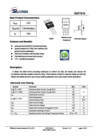
SSF7510 MOSFET Equivalente. Reemplazo. Hoja de especificaciones. Principales características
Número de Parte: SSF7510
Tipo de FET: MOSFET
Polaridad de transistor: N
ESPECIFICACIONES MÁXIMAS
Pdⓘ - Máxima
disipación de potencia: 181 W
|Vds|ⓘ - Voltaje máximo drenador-fuente: 75 V
|Vgs|ⓘ - Voltaje máximo fuente-puerta: 20 V
|Id|ⓘ - Corriente continua
de drenaje: 75 A
Tjⓘ - Temperatura máxima de unión: 175 °C
CARACTERÍSTICAS ELÉCTRICAS
trⓘ - Tiempo
de subida: 17 nS
Cossⓘ - Capacitancia de salida: 294 pF
RDSonⓘ - Resistencia estado encendido drenaje a fuente: 0.01 Ohm
Encapsulados: TO220
Búsqueda de reemplazo de SSF7510 MOSFET
- Selecciónⓘ de transistores por parámetros
SSF7510 datasheet
9.1. Size:426K silikron
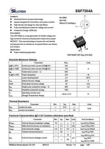
ssf7504.pdf 
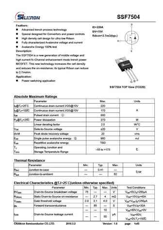
SSF7504 Feathers ID=220A Advanced trench process technology BV=75V Special designed for Convertors and power controls Rdson=2.7m (typ.) High density cell design for ultra low Rdson Fully characterized Avalanche voltage and current Avalanche Energy 100% test Description The SSF7504 is a new generation of middle voltage and high current N Channel enhancemen
9.2. Size:482K silikron
ssf7509b.pdf
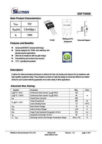
SSF7509B Main Product Characteristics VDSS 70V RDS(on) 5.3m (typ.) ID 100A Marking and Pi n TO-220 Schematic Diagram Assignment Features and Benefits Advanced MOSFET process technology Special designed for PWM, load switching and general purpose applications Ultra low on-resistance with low gate charge Fast switching and reverse body recovery
9.3. Size:417K silikron
ssf7505.pdf
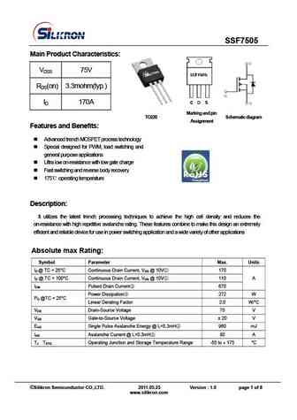
SSF7505 Main Product Characteristics VDSS 75V RDS(on) 3.3mohm(typ.) ID 170A Marking and pin TO220 Schematic diagram Assignment Features and Benefits Advanced trench MOSFET process technology Special designed for PWM, load switching and general purpose applications Ultra low on-resistance with low gate charge Fast switching and reverse body recovery 175
9.4. Size:383K silikron
ssf7508a.pdf
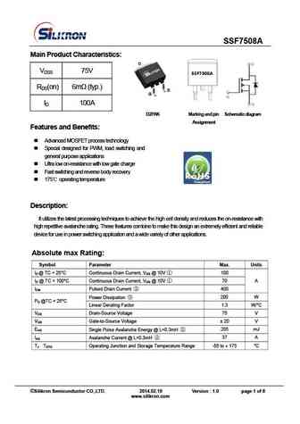
SSF7508A Main Product Characteristics VDSS 75V RDS(on) 6m (typ.) ID 100A D2PAK Marking and pin Schematic diagram Assignment Features and Benefits Advanced MOSFET process technology Special designed for PWM, load switching and general purpose applications Ultra low on-resistance with low gate charge Fast switching and reverse body recovery
9.5. Size:568K silikron
ssf7504h.pdf
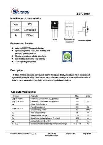
SSF7504H Main Product Characteristics VDSS 75V RDS(on) 3.9m (typ.) ID 220A Marking and p in TO- 247 Schematic diagram Assignment Features and Benefits Advanced MOSFET process technology Special designed for PWM, load switching and general purpose applications Ultra low on-resistance with low gate charge Fast switching and reverse body recover
9.6. Size:415K silikron
ssf7507.pdf

SSF7507 Main Product Characteristics VDSS 75V RDS(on) 5mohm(typ.) ID 110A TO220 Marking and pin Schematic diagram Assignment Features and Benefits Advanced trench MOSFET process technology Special designed for PWM, load switching and general purpose applications Ultra low on-resistance with low gate charge Fast switching and reverse body recovery 175
9.7. Size:396K silikron
ssf7509a.pdf
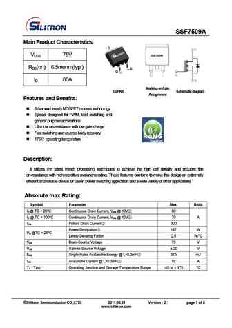
SSF7509A Main Product Characteristics VDSS 75V RDS(on) 6.5mohm(typ.) ID 80A Marking and pin D2PAK Schematic diagram Assignment Features and Benefits Advanced trench MOSFET process technology Special designed for PWM, load switching and general purpose applications Ultra low on-resistance with low gate charge Fast switching and reverse body recovery 175
9.8. Size:300K silikron
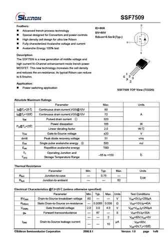
ssf7509j7.pdf
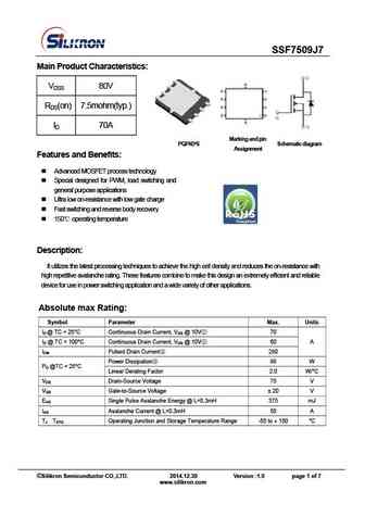
SSF7509J7 Main Product Characteristics VDSS 80V RDS(on) 7.5mohm(typ.) ID 70A Marking and pin PQFN5*6 Schematic diagram Assignment Features and Benefits Advanced MOSFET process technology Special designed for PWM, load switching and general purpose applications Ultra low on-resistance with low gate charge Fast switching and reverse body recovery
9.9. Size:470K silikron
ssf7504a7.pdf
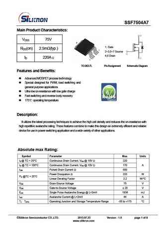
SSF7504A7 Main Product Characteristics VDSS 75V 1, Gate RDS(on) 2.5m (typ.) 2 3,5 7 Source 4,8 Drain ID 220A Schematic Diagram TO-263-7L Pin Assignment Features and Benefits Advanced MOSFET process technology Special designed for PWM, load switching and general purpose applications Ultra low on-resistance with low gate charge Fast switching
9.10. Size:513K silikron
ssf7508.pdf
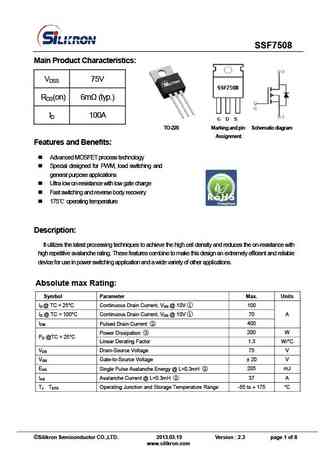
SSF7508 Main Product Characteristics VDSS 75V RDS(on) 6m (typ.) ID 100A S che mati c di agra m TO-220 Marking a nd p in Assignment Features and Benefits Advanced MOSFET process technology Special designed for PWM, load switching and general purpose applications Ultra low on-resistance with low gate charge Fast switching and reverse body recovery
9.11. Size:396K silikron
ssf7504a.pdf
SSF7504A Feathers ID=220A Advanced trench process technology BV=75V Special designed for Convertors and power controls Rdson=2.7m (typ.) High density cell design for ultra low Rdson Fully characterized Avalanche voltage and current Avalanche Energy 100% test Description The SSF7504A is a new generation of middle voltage and high current N Channel enhancem
9.12. Size:392K silikron
ssf7509.pdf
SSF7509 Feathers ID=80A Advanced trench process technology BV=80V Special designed for Convertors and power controls Rdson=6.5m (Typ.) High density cell design for ultra low Rdson Fully characterized Avalanche voltage and current Avalanche Energy 100% test Description The SSF7509 is a new generation of middle voltage and high current N Channel enhancement
Otros transistores... SSF7504H, SSF7505, SSF7507, SSF7508, SSF7508A, SSF7509A, SSF7509B, SSF7509J7, IRF840, SSF7604, SSF7607, SSF7609, SSF7610, SSF7N60, SSF7N60F, SSF7N65F, SSF7NS60D