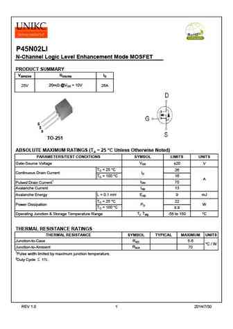
P45N02LI MOSFET Equivalente. Reemplazo. Hoja de especificaciones. Principales características
Número de Parte: P45N02LI
Tipo de FET: MOSFET
Polaridad de transistor: N
ESPECIFICACIONES MÁXIMAS
Pdⓘ - Máxima
disipación de potencia: 22 W
|Vds|ⓘ - Voltaje máximo drenador-fuente: 25 V
|Vgs|ⓘ - Voltaje máximo fuente-puerta: 20 V
|Id|ⓘ - Corriente continua
de drenaje: 26 A
Tjⓘ - Temperatura máxima de unión: 150 °C
CARACTERÍSTICAS ELÉCTRICAS
trⓘ - Tiempo
de subida: 17 nS
Cossⓘ - Capacitancia de salida: 100 pF
RDSonⓘ - Resistencia estado encendido drenaje a fuente: 0.02 Ohm
Encapsulados: TO251
Búsqueda de reemplazo de P45N02LI MOSFET
- Selecciónⓘ de transistores por parámetros
P45N02LI datasheet
..1. Size:517K unikc
p45n02li.pdf 

P45N02LI N-Channel Logic Level Enhancement Mode MOSFET PRODUCT SUMMARY V(BR)DSS RDS(ON) ID 20m @VGS = 10V 25V 26A TO-251 ABSOLUTE MAXIMUM RATINGS (TA = 25 C Unless Otherwise Noted) PARAMETERS/TEST CONDITIONS SYMBOL LIMITS UNITS VGS Gate-Source Voltage 20 V TC = 25 C 26 ID Continuous Drain Current TC = 100 C 16 A IDM 70 Pulsed Drain Current1 IAS Avalanche Cu
7.1. Size:447K unikc
p45n02ldg.pdf 

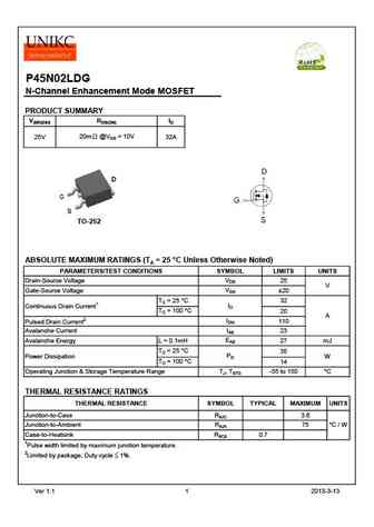
P45N02LDG N-Channel Enhancement Mode MOSFET PRODUCT SUMMARY V(BR)DSS RDS(ON) ID 25V 20m @VGS = 10V 32A TO-252 ABSOLUTE MAXIMUM RATINGS (TA = 25 C Unless Otherwise Noted) PARAMETERS/TEST CONDITIONS SYMBOL LIMITS UNITS VDS Drain-Source Voltage 25 V VGS Gate-Source Voltage 20 TC = 25 C 32 ID Continuous Drain Current1 TC = 100 C 20 A IDM 110 Pulsed Drain Curren
8.1. Size:244K utc
utp45n02.pdf 

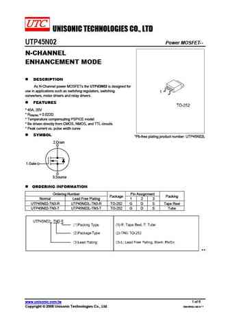
UNISONIC TECHNOLOGIES CO., LTD UTP45N02 Power MOSFET N-CHANNEL ENHANCEMENT MODE DESCRIPTION As N-Channel power MOSFETs the UTP45N02 is designed for use in applications such as switching regulators, switching converters, motor drivers and relay drivers. FEATURES * 45A, 20V * RDS(ON) = 0.022 * Temperature compensating PSPICE model * Be driven directly from CMOS, NMO
9.3. Size:89K philips
php45n03lt phb45n03lt phd45n03lt.pdf 

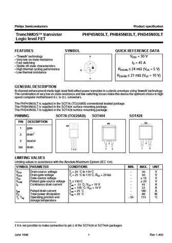
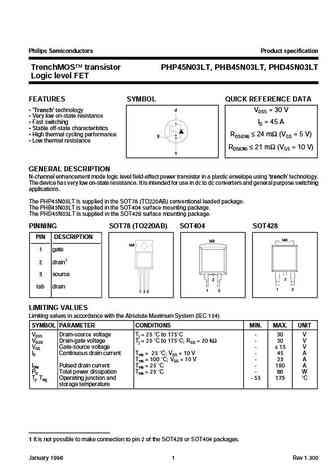
Philips Semiconductors Product specification TrenchMOS transistor PHP45N03LT, PHB45N03LT, PHD45N03LT Logic level FET FEATURES SYMBOL QUICK REFERENCE DATA Trench technology d VDSS = 30 V Very low on-state resistance Fast switching ID = 45 A Stable off-state characteristics High thermal cycling performance RDS(ON) 24 m (VGS = 5 V) g Low thermal
9.4. Size:50K philips
php45n03t 1.pdf 

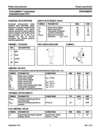
Philips Semiconductors Product specification TrenchMOS transistor PHP45N03T Standard level FET GENERAL DESCRIPTION QUICK REFERENCE DATA N-channel enhancement mode SYMBOL PARAMETER MAX. UNIT standard level field-effect power transistor in a plastic envelope using VDS Drain-source voltage 30 V trench technology. The device ID Drain current (DC) 45 A features very low on-state r
9.5. Size:295K philips
php45n03lt-06.pdf 

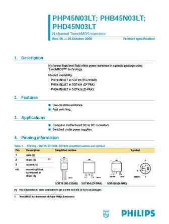
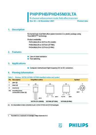
PHP45N03LT; PHB45N03LT; PHD45N03LT N-channel TrenchMOS transistor Rev. 06 05 October 2000 Product specification 1. Description N-channel logic level field-effect power transistor in a plastic package using TrenchMOS 1 technology. Product availability PHP45N03LT in SOT78 (TO-220AB) PHB45N03LT in SOT404 (D2-PAK) PHD45N03LT in SOT428 (D-PAK). 2. Features Low on-state resistance
9.6. Size:45K philips
php45n03lt 2.pdf 

Philips Semiconductors Product specification TrenchMOS transistor PHP45N03LT, PHB45N03LT, PHD45N03LT Logic level FET FEATURES SYMBOL QUICK REFERENCE DATA Trench technology d VDSS = 30 V Very low on-state resistance Fast switching ID = 45 A Stable off-state characteristics High thermal cycling performance RDS(ON) 24 m (VGS = 5 V) g Low thermal
9.7. Size:113K philips
php45n03lta phb45n03lta phd45n03lta.pdf 

PHP/PHB/PHD45N03LTA N-channel enhancement mode field-effect transistor Rev. 02 02 November 2001 Product data 1. Description N-channel logic level field-effect power transistor in a plastic package using TrenchMOS 1 technology. Product availability PHP45N03LTA in SOT78 (TO-220AB) PHB45N03LTA in SOT404 (D2-PAK) PHD45N03LTA in SOT428 (D-PAK). 2. Features Low on-state resistance
9.8. Size:295K philips
php45n03lt.pdf 

PHP45N03LT; PHB45N03LT; PHD45N03LT N-channel TrenchMOS transistor Rev. 06 05 October 2000 Product specification 1. Description N-channel logic level field-effect power transistor in a plastic package using TrenchMOS 1 technology. Product availability PHP45N03LT in SOT78 (TO-220AB) PHB45N03LT in SOT404 (D2-PAK) PHD45N03LT in SOT428 (D-PAK). 2. Features Low on-state resistance
9.9. Size:104K renesas
np45n06puk np45n06vuk.pdf 

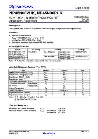
Preliminary Data Sheet NP45N06VUK, NP45N06PUK R07DS0953EJ0100 60 V 45 A N-channel Power MOS FET Rev.1.00 Application Automotive Nov 20, 2012 Description These products are N-channel MOS Field Effect Transistors designed for high current switching applications. Features Super low on-state resistance RDS(on) = 9.6 m MAX. (VGS = 10 V, ID = 23 A) Low Ciss Ci
9.10. Size:372K fairchild semi
rfg45n06 rfp45n06 rf1s45n06sm.pdf 

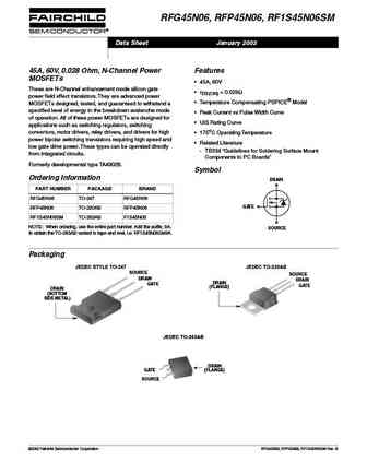
RFG45N06, RFP45N06, RF1S45N06SM Data Sheet January 2002 45A, 60V, 0.028 Ohm, N-Channel Power Features MOSFETs 45A, 60V These are N-Channel enhancement mode silicon gate rDS(ON) = 0.028 power field effect transistors. They are advanced power Temperature Compensating PSPICE Model MOSFETs designed, tested, and guaranteed to withstand a specified level of energy in the
9.11. Size:52K vishay
sup45n05.pdf 

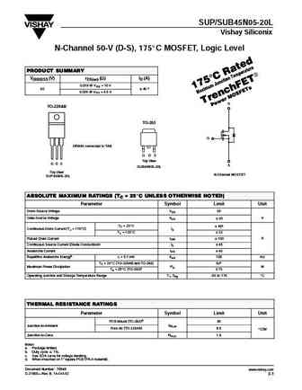
SUP/SUB45N05-20L Vishay Siliconix N-Channel 50-V (D-S), 175_C MOSFET, Logic Level PRODUCT SUMMARY V(BR)DSS (V) rDS(on) (W) ID (A) 0.018 @ VGS = 10 V 50 "45 a " 0.020 @ VGS = 4.5 V D TO-220AB TO-263 G DRAIN connected to TAB G D S Top View G D S S SUB45N05-20L Top View N-Channel MOSFET SUP45N05-20L ABSOLUTE MAXIMUM RATINGS (TC = 25_C UNLESS OTHERWISE NOTED) Parameter Symbol
9.12. Size:41K vishay
sub45n05-20l sup45n05-20l.pdf 

SUP/SUB45N05-20L Vishay Siliconix N-Channel 50-V (D-S), 175_C MOSFET, Logic Level PRODUCT SUMMARY V(BR)DSS (V) rDS(on) (W) ID (A) 0.018 @ VGS = 10 V 50 "45 a " 0.020 @ VGS = 4.5 V D TO-220AB TO-263 G DRAIN connected to TAB G D S Top View G D S S SUB45N05-20L Top View N-Channel MOSFET SUP45N05-20L ABSOLUTE MAXIMUM RATINGS (TC = 25_C UNLESS OTHERWISE NOTED) Parameter Symbol
9.13. Size:45K vishay
sup45n03-13l.pdf 

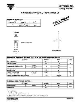
SUP45N03-13L Vishay Siliconix N-Channel 30-V (D-S), 175_C MOSFET PRODUCT SUMMARY V(BR)DSS (V) rDS(on) (W) ID (A) 0.013 @ VGS = 10 V 45a 30 0.02 @ VGS = 4.5 V 45a D TO-220AB G DRAIN connected to TAB G D S S Top View N-Channel MOSFET SUP45N03-13L ABSOLUTE MAXIMUM RATINGS (TC = 25_C UNLESS OTHERWISE NOTED) Parameter Symbol Limit Unit Drain-Source Voltage VDS 30 Gate-Source Volt
9.14. Size:159K infineon
ipb45n06s4-09 ipi45n06s4-09 ipp45n06s4-09.pdf 

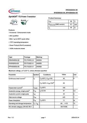
IPB45N06S4-09 IPI45N06S4-09, IPP45N06S4-09 OptiMOS -T2 Power-Transistor Product Summary V 60 V DS R (SMD version) 9.2 m DS(on),max I 45 A D Features N-channel - Enhancement mode AEC qualified MSL1 up to 260 C peak reflow 175 C operating temperature Green Product (RoHS compliant) 100% Avalanche tested Type Package Marking IPB45N06S4-09 PG-TO263-
9.15. Size:170K infineon
ipb45n06s4l-08 ipi45n06s4l-08 ipp45n06s4l-08 ipp45n06s4l ipb45n06s4l ipi45n06s4l-08.pdf 

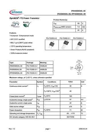
IPB45N06S4L-08 IPI45N06S4L-08, IPP45N06S4L-08 OptiMOS -T2 Power-Transistor Product Summary V 60 V DS R (SMD version) 7.9 m DS(on),max I 45 A D Features N-channel - Enhancement mode PG-TO263-3-2 PG-TO262-3-1 PG-TO220-3-1 AEC Q101 qualified MSL1 up to 260 C peak reflow 175 C operating temperature Green Product (RoHS compliant) 100% Avalanche tested
9.16. Size:159K infineon
ipp45n04s4l-08 ipb45n04s4l-08 ipi45n04s4l-08.pdf 

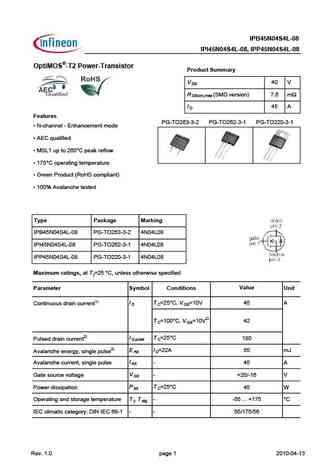
IPB45N04S4L-08 IPI45N04S4L-08, IPP45N04S4L-08 OptiMOS -T2 Power-Transistor Product Summary V 40 V DS R (SMD version) 7.6 m DS(on),max I 45 A D Features PG-TO263-3-2 PG-TO262-3-1 PG-TO220-3-1 N-channel - Enhancement mode AEC qualified MSL1 up to 260 C peak reflow 175 C operating temperature Green Product (RoHS compliant) 100% Avalanche tested Typ
9.17. Size:81K onsemi
ntb45n06lg ntp45n06l ntp45n06l ntb45n06l.pdf 

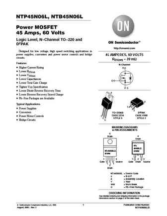
NTP45N06L, NTB45N06L Power MOSFET 45 Amps, 60 Volts Logic Level, N-Channel TO-220 and D2PAK http //onsemi.com Designed for low voltage, high speed switching applications in power supplies, converters and power motor controls and bridge 45 AMPERES, 60 VOLTS circuits. RDS(on) = 28 mW Features N-Channel Higher Current Rating D Lower RDS(on) Lower VDS(on) Lower Capa
9.18. Size:81K onsemi
ntb45n06g ntp45n06 ntp45n06 ntb45n06.pdf 

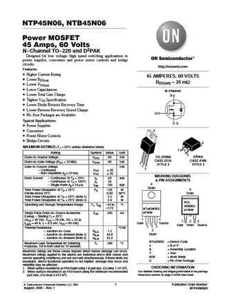
NTP45N06, NTB45N06 Power MOSFET 45 Amps, 60 Volts N-Channel TO-220 and D2PAK Designed for low voltage, high speed switching applications in power supplies, converters and power motor controls and bridge circuits. http //onsemi.com Features Higher Current Rating 45 AMPERES, 60 VOLTS Lower RDS(on) RDS(on) = 26 mW Lower VDS(on) Lower Capacitances N-Channel Lower
9.19. Size:81K onsemi
ntp45n06l ntb45n06l.pdf 

NTP45N06L, NTB45N06L Power MOSFET 45 Amps, 60 Volts Logic Level, N-Channel TO-220 and D2PAK http //onsemi.com Designed for low voltage, high speed switching applications in power supplies, converters and power motor controls and bridge 45 AMPERES, 60 VOLTS circuits. RDS(on) = 28 mW Features N-Channel Higher Current Rating D Lower RDS(on) Lower VDS(on) Lower Capa
9.20. Size:202K intersil
rfp45n06le rf1s45n06lesm.pdf 

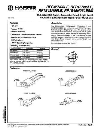
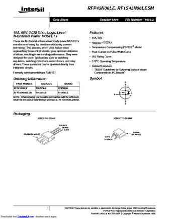
RFP45N06LE, RF1S45N06LESM Data Sheet October 1999 File Number 4076.2 45A, 60V, 0.028 Ohm, Logic Level Features N-Channel Power MOSFETs 45A, 60V These are N-Channel enhancement mode power MOSFETs rDS(ON) = 0.028 manufactured using the latest manufacturing process Temperature Compensating PSPICE Model technology. This process, which uses feature sizes approaching those
9.21. Size:488K unikc
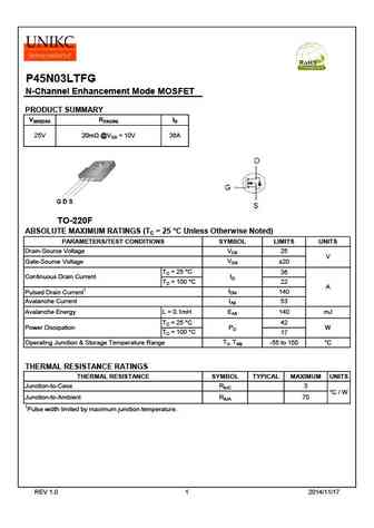
p45n03ltfg.pdf 

P45N03LTFG N-Channel Enhancement Mode MOSFET PRODUCT SUMMARY V(BR)DSS RDS(ON) ID 20m @VGS = 10V 25V 36A TO-220F ABSOLUTE MAXIMUM RATINGS (TC = 25 C Unless Otherwise Noted) PARAMETERS/TEST CONDITIONS SYMBOL LIMITS UNITS VDS Drain-Source Voltage 25 V VGS Gate-Source Voltage 20 TC = 25 C 36 ID Continuous Drain Current TC = 100 C 22 A IDM 140 Pulsed Drain Curr
9.22. Size:263K shantou-huashan
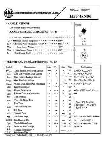
hfp45n06.pdf 

N-Channel MOSFET Shantou Huashan Electronic Devices Co.,Ltd. HFP45N06 APPLICATIONSL TO-220 Low Voltage high-Speed Switching. ABSOLUTE MAXIMUM RATINGS Ta=25 Tstg Storage Temperature -55 175 1 G Tj Operating Junction Temperature 150 2 D PD Allowable Power Dissipation Tc
9.23. Size:177K tysemi
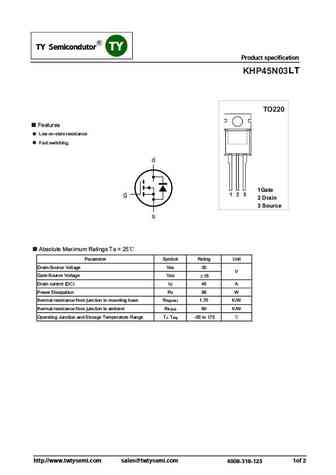
khp45n03lt.pdf 

SMDTypee Ior DIP Type Tra n s is tICs SMD Type SMD Type SMDType C Typ SMD DIP Type IC Product specification KHP45N03LT TO220 Features Low on-state resistance Fast switching. 1Gate 2Drain 3Source Absolute Maximum Ratings Ta = 25 Parameter Symbol Rating Unit Drain-Source Voltage VDS 30 V Gate-Source Voltage VGS 15 Drain current (DC) ID 45 A Power Dissipation PD 86 W therma
9.24. Size:1057K semihow
hrp45n06k.pdf 

December 2014 BVDSS = 60 V RDS(on) typ = 3.7m HRP45N06K ID = 150 A 60V N-Channel Trench MOSFET TO-220 FEATURES Originative New Design Superior Avalanche Rugged Technology 1 2 3 Excellent Switching Characteristics 1.Gate 2. Drain 3. Source Unrivalled Gate Charge 120 nC (Typ.) Extended Safe Operating Area Lower RDS(ON) 3.7 m (Typ.
9.25. Size:903K semihow
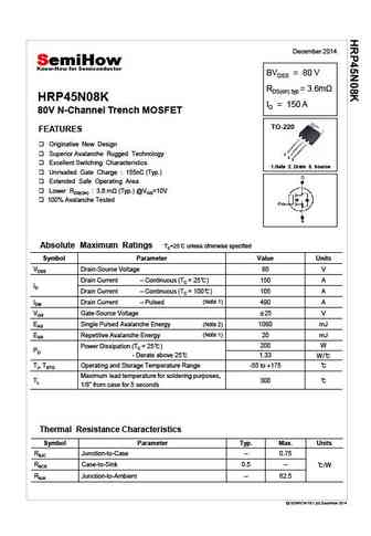
hrp45n08k.pdf 

December 2014 BVDSS = 80 V RDS(on) typ = 3.6m HRP45N08K ID = 150 A 80V N-Channel Trench MOSFET TO-220 FEATURES Originative New Design Superior Avalanche Rugged Technology 1 2 3 Excellent Switching Characteristics 1.Gate 2. Drain 3. Source Unrivalled Gate Charge 155nC (Typ.) Extended Safe Operating Area Lower RDS(ON) 3.6 m (Typ.)
Otros transistores... PZP103BYB
, TD304BH
, TD357EG
, TD381BA
, TD422BL
, P4506BD
, P4506BV
, P45N02LDG
, IRFP460
, P45N03LTFG
, P0460AD
, P0460AI
, P0460AS
, P0460AT
, P0460ATF
, P0460BTF
, P0460BTFS
.
History: 2SK2915
