P0465CS MOSFET Equivalente. Reemplazo. Hoja de especificaciones. Principales características
Número de Parte: P0465CS
Tipo de FET: MOSFET
Polaridad de transistor: N
ESPECIFICACIONES MÁXIMAS
Pdⓘ - Máxima disipación de potencia: 71 W
|Vds|ⓘ - Voltaje máximo drenador-fuente: 650 V
|Vgs|ⓘ - Voltaje máximo fuente-puerta: 30 V
|Id|ⓘ - Corriente continua de drenaje: 4 A
Tjⓘ - Temperatura máxima de unión: 150 °C
CARACTERÍSTICAS ELÉCTRICAS
trⓘ - Tiempo de subida: 60 nS
Cossⓘ - Capacitancia de salida: 49 pF
RDSonⓘ - Resistencia estado encendido drenaje a fuente: 2.6 Ohm
Encapsulados: TO263
Búsqueda de reemplazo de P0465CS MOSFET
- Selecciónⓘ de transistores por parámetros
P0465CS datasheet
p0465cs.pdf
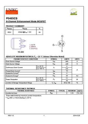
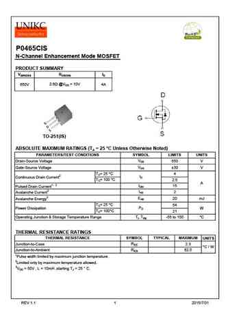
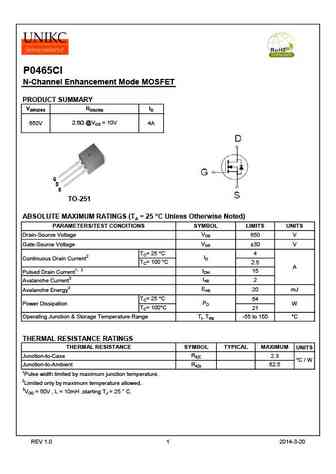
P0465CS N-Channel Enhancement Mode MOSFET PRODUCT SUMMARY V(BR)DSS RDS(ON) ID 2.6m @VGS = 10V 650V 4A TO-263 ABSOLUTE MAXIMUM RATINGS (TA = 25 C Unless Otherwise Noted) PARAMETERS/TEST CONDITIONS SYMBOL LIMITS UNITS VDS Drain-Source Voltage 650 V VGS Gate-Source Voltage 30 V TC= 25 C 4 ID Continuous Drain Current TC= 100 C 2.5 A IDM 15 Pulsed Drain Current1
p0465cd.pdf
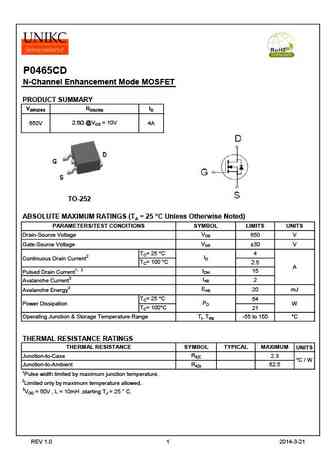
P0465CD N-Channel Enhancement Mode MOSFET PRODUCT SUMMARY V(BR)DSS RDS(ON) ID 2.6 @VGS = 10V 650V 4A TO-252 ABSOLUTE MAXIMUM RATINGS (TA = 25 C Unless Otherwise Noted) PARAMETERS/TEST CONDITIONS SYMBOL LIMITS UNITS VDS Drain-Source Voltage 650 V VGS Gate-Source Voltage 30 V TC= 25 C 4 ID Continuous Drain Current2 TC= 100 C 2.5 A IDM 15 Pulsed Drain Current1
p0465ct.pdf
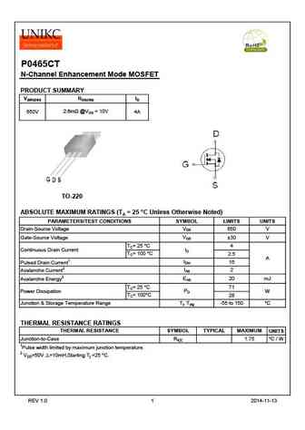
P0465CT N-Channel Enhancement Mode MOSFET PRODUCT SUMMARY V(BR)DSS RDS(ON) ID 2.6m @VGS = 10V 650V 4A TO-220 ABSOLUTE MAXIMUM RATINGS (TA = 25 C Unless Otherwise Noted) PARAMETERS/TEST CONDITIONS SYMBOL LIMITS UNITS VDS Drain-Source Voltage 650 V VGS Gate-Source Voltage 30 V TC= 25 C 4 ID Continuous Drain Current TC= 100 C 2.5 A IDM 15 Pulsed Drain Current1
p0465ctf-s.pdf
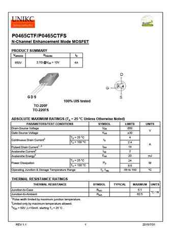
P0465CTF/P0465CTFS N-Channel Enhancement Mode MOSFET PRODUCT SUMMARY V(BR)DSS RDS(ON) ID 2.7 @VGS = 10V 650V 4A 100% UIS tested TO-220F TO-220FS ABSOLUTE MAXIMUM RATINGS (TA = 25 C Unless Otherwise Noted) PARAMETERS/TEST CONDITIONS SYMBOL LIMITS UNITS VDS Drain-Source Voltage 650 V VGS Gate-Source Voltage 30 TC = 25 C 4 ID Continuous Drain Current2 TC = 100 C
Otros transistores... P0460EIS , P0460ETF , P0465AD , P0465ATF , P0465ATFS , P0465CD , P0465CI , P0465CIS , IRF9540 , P0465CT , P0465CTF , P0465CTFS , P0470ATF , P0470ATFS , P0502CEA , P0510AT , P0550AD .
History: UPA1901 | P0465CIS | APM4317K
History: UPA1901 | P0465CIS | APM4317K
🌐 : EN ES РУ

Liste
Recientemente añadidas las descripciónes de los transistores:
MOSFET: AUN084N10 | AUN065N10 | AUN063N10 | AUN062N08BG | AUN060N08AG | AUN053N10 | AUN050N08BGL | AUN045N085 | AUN042N055 | AUN036N10 | AUD069N10A | AUD062N08BG | AUD060N08AG | AUD060N055 | AUD056N08BGL | AUB062N08BG
Popular searches
tip36c | bd139 transistor | irf840 datasheet | ge10001 | irf830 | irfp450 | mj21193 | s9014 transistor