APM4550J MOSFET Equivalente. Reemplazo. Hoja de especificaciones. Principales características
Número de Parte: APM4550J
Tipo de FET: MOSFET
Polaridad de transistor: NP
ESPECIFICACIONES MÁXIMAS
Pdⓘ - Máxima disipación de potencia: 2.5 W
|Vds|ⓘ - Voltaje máximo drenador-fuente: 30 V
|Vgs|ⓘ - Voltaje máximo fuente-puerta: 20 V
|Id|ⓘ - Corriente continua de drenaje: 8(7) A
Tjⓘ - Temperatura máxima de unión: 150 °C
CARACTERÍSTICAS ELÉCTRICAS
RDSonⓘ - Resistencia estado encendido drenaje a fuente: 0.0275(0.05) Ohm
Encapsulados: DIP8
Búsqueda de reemplazo de APM4550J MOSFET
- Selecciónⓘ de transistores por parámetros
APM4550J datasheet
apm4550j.pdf
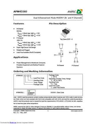
APM4550J Dual Enhancement Mode MOSFET (N- and P-Channel) Features Pin Description N-Channel 30V/8A, RDS(ON) = 20m (typ.) @ VGS = 10V RDS(ON) = 30m (typ.) @ VGS = 4.5V P-Channel Top View of DIP - 8 -30V/-7A, RDS(ON) = 40m (typ.) @ VGS = -10V D1 D1 S2 RDS(ON) = 62m (typ.) @ VGS = -4.5V Super High Dense Cell Design Reliable and Rugged Lead Free Available (RoHS Compl
apm4550k.pdf
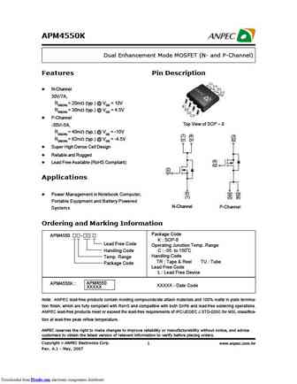
APM4550K Dual Enhancement Mode MOSFET (N- and P-Channel) Features Pin Description N-Channel 30V/7A, RDS(ON) = 20m (typ.) @ VGS = 10V RDS(ON) = 30m (typ.) @ VGS = 4.5V P-Channel Top View of SOP - 8 -30V/-5A, RDS(ON) = 40m (typ.) @ VGS = -10V (7) (8) (3) RDS(ON) = 62m (typ.) @ VGS = -4.5V D1 D1 S2 Super High Dense Cell Design Reliable and Rugged (4) Lead Free Av
apm4550kc.pdf
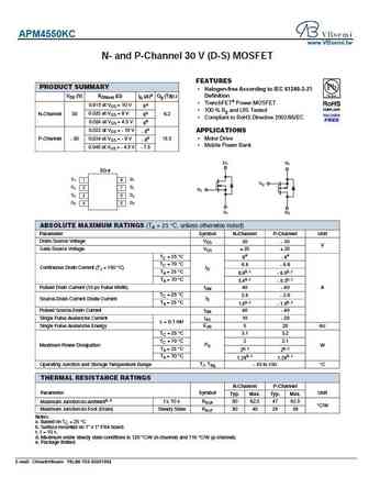
APM4550KC www.VBsemi.tw N- and P-Channel 30 V (D-S) MOSFET FEATURES PRODUCT SUMMARY Halogen-free According to IEC 61249-2-21 VDS (V) RDS(on) ( ) Definition ID (A)a Qg (Typ.) TrenchFET Power MOSFET 0.018 at VGS = 10 V 8e 100 % Rg and UIS Tested N-Channel 30 0.020 at VGS = 8 V 8e 6.2 Compliant to RoHS Directive 2002/95/EC 0.024 at VGS = 4.5 V 8e 0.032 at VG
apm4552k.pdf
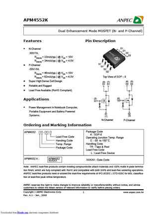
APM4552K Dual Enhancement Mode MOSFET (N- and P-Channel) Features Pin Description D1 N-Channel D1 D2 30V/7A, D2 RDS(ON) = 23m (typ.) @ VGS = 10V RDS(ON) = 34m (typ.) @ VGS = 4.5V S1 P-Channel G1 -30V/-5A, S2 G2 RDS(ON) = 46m (typ.) @ VGS =-10V RDS(ON) = 62m (typ.) @ VGS =-4.5V Top View of SOP - 8 Super High Dense Cell Design (6) (5) (8) (7) D2 D2 D1 D1
Otros transistores... APM4532 , APM4532K , APM4534K , APM4536K , APM4538K , APM4542K , APM4548AK , APM4548K , IRF9540N , APM4550K , APM4552K , 2SK3096 , APM4568J , APM4568K , APM4588K , APM4800 , APM4804K .
History: APM4548K
History: APM4548K
🌐 : EN ES РУ

Liste
Recientemente añadidas las descripciónes de los transistores:
MOSFET: AUB062N08BG | AUB060N08AG | AUB056N10 | AUB056N08BGL | AUB050N085 | AUB050N055 | AUB045N12 | AUB045N10BT | AUB039N10 | AUB034N10 | AUB033N08BG | AUB026N085 | AUA062N08BG | AUA060N08AG | AUA056N08BGL | AUA039N10
Popular searches
a1023 datasheet | 2sc1080 | 2sb618 | 2sc1328 | 2sc1845 transistor | a933 transistor datasheet | a1633 transistor | 2sa844