2015 MOSFET Equivalente. Reemplazo. Hoja de especificaciones. Principales características
Número de Parte: 2015
Tipo de FET: MOSFET
Polaridad de transistor: P
ESPECIFICACIONES MÁXIMAS
Pdⓘ - Máxima
disipación de potencia: 1.25 W
|Vds|ⓘ - Voltaje máximo drenador-fuente: 20 V
|Vgs|ⓘ - Voltaje máximo fuente-puerta: 8 V
|Id|ⓘ - Corriente continua
de drenaje: 2.8 A
Tjⓘ - Temperatura máxima de unión: 150 °C
CARACTERÍSTICAS ELÉCTRICAS
trⓘ - Tiempo
de subida: 6.4 nS
Cossⓘ - Capacitancia de salida: 62 pF
RDSonⓘ - Resistencia estado encendido drenaje a fuente: 0.08 Ohm
Encapsulados: SOT23
Búsqueda de reemplazo de 2015 MOSFET
- Selecciónⓘ de transistores por parámetros
2015 datasheet
..1. Size:392K shenzhen
2015.pdf 

Shenzhen Tuofeng Semiconductor Technology Co., Ltd 2015 Single P-Channel, -20V, -2.4A, Power MOSFET VDS (V) Rds(on) ( ) 0.081@ VGS= 4.5V -20 0.103@ VGS= 2.5V SOT-23 Descriptions D The 2015 is P-Channel enhancement 3 MOS Field Effect Transistor. Uses advanced trench technology and design to provide excellent RDS (ON) with low gate charge. This device is suitable for use in DC
0.2. Size:62K philips
lwe2015r 2.pdf
DISCRETE SEMICONDUCTORS DATA SHEET LWE2015R NPN microwave power transistor 1997 Feb 19 Product specification Supersedes data of November 1994 File under Discrete Semiconductors, SC15 Philips Semiconductors Product specification NPN microwave power transistor LWE2015R FEATURES PINNING - SOT446A Interdigitated structure provides high emitter efficiency PIN DESCRIPTION Diffus
0.3. Size:28K sanyo
fts2015.pdf
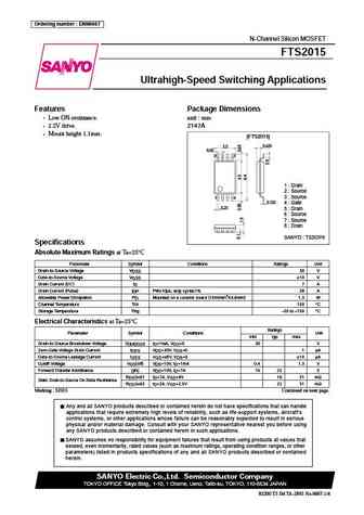
Ordering number ENN6667 FTS2015 N-Channel Silicon MOSFET FTS2015 Ultrahigh-Speed Switching Applications Features Package Dimensions Low ON-resistance. unit mm 2.5V drive. 2147A Mount height 1.1mm. [FTS2015] 3.0 0.425 0.65 8 5 1 Drain 2 Source 3 Source 1 4 0.125 4 Gate 0.25 5 Drain 6 Source 7 Source 8 Drain SANYO TSSOP8 Specifications A
0.4. Size:41K sanyo
ftd2015.pdf
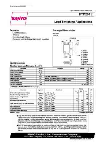
Ordering number ENN6393 N-Channel Silicon MOSFET FTD2015 Load Switching Applications Features Package Dimensions Low ON resistance. unit mm 4V drive. 2155A Mounting height 1.1mm. [FTD2015] Composite type, facilitating high-density mounting. 3.0 0.425 0.65 8 5 1 Drain1 2 Source1 1 4 3 Source1 0.125 4 Gate1 0.25 5 Gate2 6 Source2 7 Source2 8
0.5. Size:49K sanyo
2sa2015 2sc5568.pdf
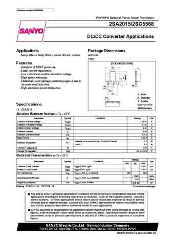
Ordering number ENN6308 PNP/NPN Epitaxial Planar Silicon Transistors 2SA2015/2SC5568 DC/DC Converter Applications Applications Package Dimensions Relay drivers, lamp drivers, motor drivers, strobes. unit mm 2163 Features [2SA2015/2SC5568] 4.5 Adoption of MBIT processes. 1.6 1.5 Large current capacitance. Low collector-to-emitter saturation voltage. High-speed sw
0.6. Size:489K diodes
dmn2015ufde.pdf
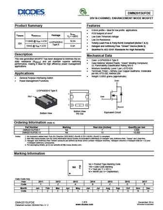
DMN2015UFDE 20V N-CHANNEL ENHANCEMENT MODE MOSFET Product Summary Features 0.6mm profile ideal for low profile applications PCB footprint of 4mm2 ID max V(BR)DSS RDS(ON) max Package TA = +25 C Low Gate Threshold Voltage Low On-Resistance 11.6m @ VGS = 4.5V 10.5A U-DFN2020-6 Totally Lead-Free & Fully RoHS Compliant (Notes 1 & 2) 20V Type E
0.7. Size:33K panasonic
2sk2015.pdf

Power F-MOS FETs 2SK2015 2SK2015 Silicon N-Channel Power F-MOS Unit mm 6.5 0.1 Features 5.3 0.1 Low ON-resistance RDS(on) RDS(on)1= 0.7 (typ) 4.35 0.1 3.0 0.1 High-speed switching tf= 36ns(typ) No secondary breakdown For low-voltage drive(VGS= 4V) Taping supply possible Applications 1.0 0.1 DC-DC converter 0.85 0.1 0.75 0.1 0.5 0.1 Non-contact relay
0.8. Size:72K jmnic
2sd2015.pdf
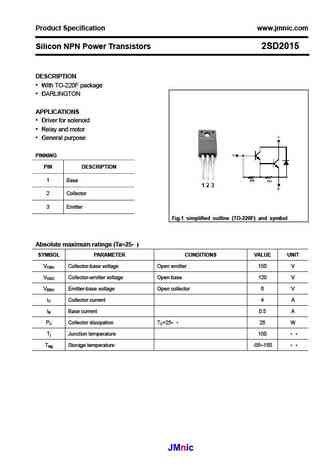
Product Specification www.jmnic.com Silicon NPN Power Transistors 2SD2015 DESCRIPTION With TO-220F package DARLINGTON APPLICATIONS Driver for solenoid Relay and motor General purpose PINNING PIN DESCRIPTION 1 Base 2 Collector 3 Emitter Fig.1 simplified outline (TO-220F) and symbol Absolute maximum ratings (Ta=25 ) SYMBOL PARAMETER CONDITIONS VALUE UNIT
0.9. Size:36K kec
kta2015.pdf
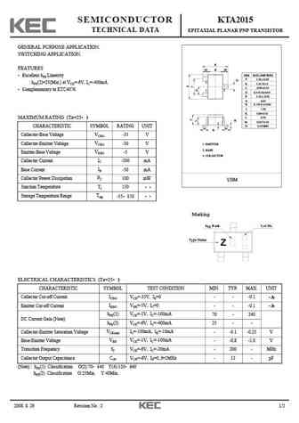
SEMICONDUCTOR KTA2015 TECHNICAL DATA EPITAXIAL PLANAR PNP TRANSISTOR GENERAL PURPOSE APPLICATION. SWITCHING APPLICATION. E FEATURES M B M DIM MILLIMETERS Excellent hFE Linearity _ A + 2.00 0.20 D 2 hFE(2)=25(Min.) at VCE=-6V, IC=-400mA. _ + B 1.25 0.15 _ + C 0.90 0.10 Complementary to KTC4076. 3 1 D 0.3+0.10/-0.05 _ E + 2.10 0.20 G 0.65 H 0.15+0.1/-0.06 J 1.3
0.10. Size:26K sanken-ele
2sd2015.pdf
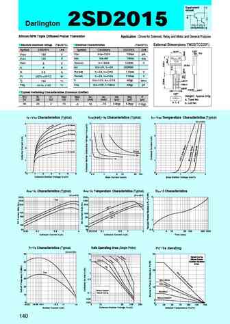
Equivalent C circuit B Darlington 2SD2015 (3k ) (500 ) E Silicon NPN Triple Diffused Planar Transistor Application Driver for Solenoid, Relay and Motor and General Purpose Absolute maximum ratings (Ta=25 C) Electrical Characteristics (Ta=25 C) External Dimensions FM20(TO220F) Symbol Conditions 2SD2015 Symbol 2SD2015 Unit Unit 0.2 4.2 0.2 10.1 c0.5 2.8 ICBO VCB=150V
0.11. Size:510K htsemi
kta2015.pdf
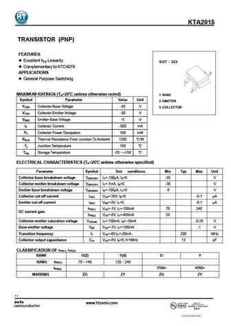
KTA2015 TRANSISTOR (PNP) FEATURES Excellent hFE Linearity SOT 323 Complementary to KTC4076 APPLICATIONS General Purpose Switching MAXIMUM RATINGS (Ta=25 unless otherwise noted) 1. BASE Symbol Parameter Value Unit 2. EMITTER V Collector-Base Voltage -35 V CBO 3. COLLECTOR VCEO Collector-Emitter Voltage -30 V V Emitter-Base Voltage -5 V EBO I Col
0.12. Size:66K wietron
kta2015.pdf
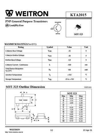
KTA2015 PNP General Purpose Transistors 3 P b Lead(Pb)-Free 1 2 SOT-323 MAXIMUM RATINGS(Ta=25 C) Rating Symbol Value Unit VCBO Collector-Base Voltage -35 V Collector-Emitter Voltage VCEO -30 V VEBO Emitter-Base Voltage -5.0 V IC Collector Current - Continuous -500 mA Total Device Dissipation PD 100 mW T =25 C A Tj C Junction Temperature +150 Tstg Storage Temperatur
0.13. Size:807K willsemi
wpm2015.pdf
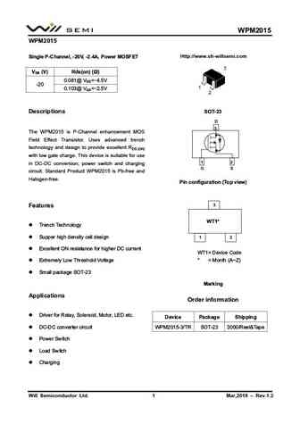
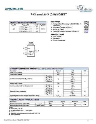
WPM2015 WPM2015 Http //www.sh-willsemi.com Single P-Channel, -20V, -2.4A, Power MOSFET VDS (V) Rds(on) ( ) 0.081@ VGS= 4.5V -20 0.103@ VGS= 2.5V SOT-23 Descriptions D 3 The WPM2015 is P-Channel enhancement MOS Field Effect Transistor. Uses advanced trench technology and design to provide excellent RDS (ON) with low gate charge. This device is suitable for use 12 in DC-D
0.14. Size:531K silikron
sspl2015f.pdf
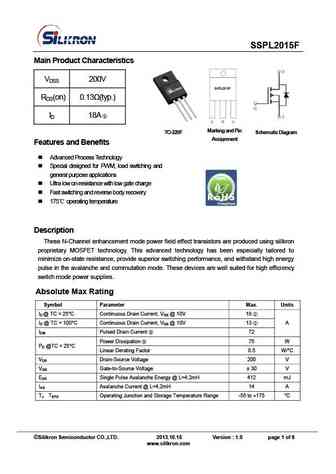
SSPL2015F Main Product Characteristics VDSS 200V RDS(on) 0.13 (typ.) ID 18A Marking and P in Schematic Diagram TO-220F Assignment Features and Benefits Advanced Process Technology Special designed for PWM, load switching and general purpose applications Ultra low on-resistance with low gate charge Fast switching and reverse body recovery 17
0.15. Size:563K silikron
sspl2015d.pdf
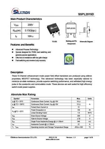
SSPL2015D Main Product Characteristics VDSS 200V RDS(on) 0.13 (typ.) ID 18A Schematic Diagram TO-252 Marking a nd P in Assignment Features and Benefits Advanced Process Technology Special designed for PWM, load switching and general purpose applications Ultra low on-resistance with low gate charge Fast switching and reverse body recovery Descri
0.16. Size:571K silikron
sspl2015.pdf
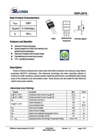
SSPL2015 Main Product Characteristics VDSS 200V RDS(on) 0.13ohm(typ.) ID 18A Mar ki ng a nd p in Sche ma ti c di agr a m TO220 Assignment Features and Benefits Advanced Process Technology Special designed for PWM, load switching and general purpose applications Ultra low on-resistance with low gate charge Fast switching and reverse body recovery
0.17. Size:105K china
lj2015-52.pdf
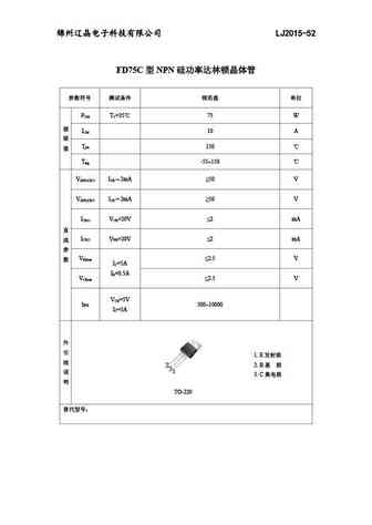
LJ2015-52 FD75C NPN P T =25 75 W CM C I 10 A CM T 150 jm T -55 150 stg V I 2mA 50 V (BR)CBO CB V I 2mA 50 V (BR)CEO CE I V =20V 2 mA CBO CB I V =20V 2 mA CEO EB V 2.5 V BEsat I =5A C I =0.5A B
0.18. Size:70K china
cs7456 lj2015-53.pdf
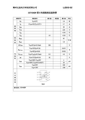
LJ2015-53 CS7456DP N P T =25 1.9 W D A I V =10V,T =25 5.7 A D GS A I 40 A DM V 20 V GS T +150 jm T -55 +150 stg R 65 thJA /W R 1.8 thJC BV V =0V,I =0.25mA 100 V DSS GS D V =10V,I =9.3A 0.025
0.19. Size:84K tysemi
wpm2015.pdf
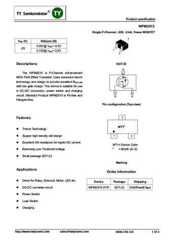
Product specification WPM2015 Single P-Channel, -20V, -2.4A, Power MOSFET VDS (V) Rds(on) ( ) 0.081@ VGS= 4.5V -20 0.103@ VGS= 2.5V SOT-23 Descriptions D The WPM2015 is P-Channel enhancement 3 MOS Field Effect Transistor. Uses advanced trench technology and design to provide excellent RDS (ON) with low gate charge. This device is suitable for use in DC-DC conversion, power s
0.20. Size:1569K kexin
wpm2015.pdf
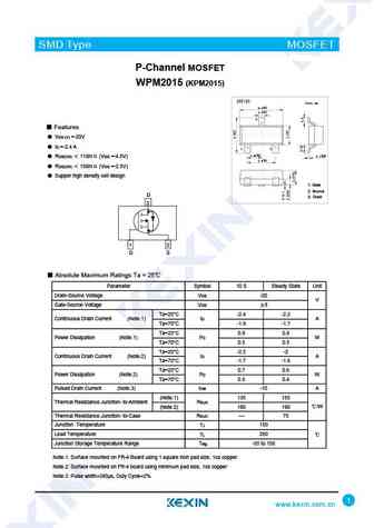
SMD Type MOSFET P-Channel MOSFET WPM2015 (KPM2015) SOT-23 Unit mm +0.1 2.9 -0.1 +0.1 0.4 -0.1 3 Features VDS (V) =-20V ID =-2.4 A 1 2 +0.1 +0.05 0.95-0.1 0.1-0.01 RDS(ON) 110m (VGS =-4.5V) +0.1 1.9-0.1 RDS(ON) 150m (VGS =-2.5V) Supper high density cell design 1. Gate 2. Source D 3. Drain 3 1 2 G S Absolute Maximum Rating
0.21. Size:1010K kexin
kta2015.pdf
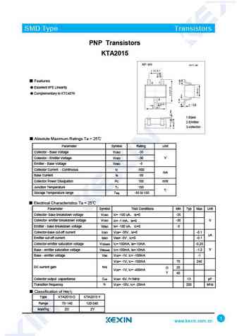
SMD Type Transistors PNP Transistors KTA2015 Features Excellent hFE Linearity Complementary to KTC4076 1.Base 2.Emitter 3.collector Absolute Maximum Ratings Ta = 25 Parameter Symbol Rating Unit Collector - Base Voltage VCBO -35 Collector - Emitter Voltage VCEO -30 V Emitter - Base Voltage VEBO -5 Collector Current - Continuous IC -500 mA Base Current IB
0.22. Size:284K msksemi
wpm2015-ms.pdf

www.msksemi.com WPM2015-MS Semiconductor Compiance APPLICATION Load Switch for Portable Devices DC/DC Converter FEATURE TrenchFET Power MOSFET I V(BR)DSS RDS(on)MAX D 90 m @-4.5V -20 V -3 A 110 m @-2.5V 1. GATE 2. SOURCE 3. DRAIN SOT-23-3L Maximum ratings (Ta=25 unless otherwise noted) Parameter Symbol Value Unit Drain-Source Voltage V -20 DS V Gate-So
0.23. Size:659K cn tuofeng
tf2015.pdf
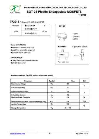
SHENZHEN TUOFENG SEMICONDUCTOR TECHNOLOGY CO.,LTD SOT-23 Plastic-Encapsulate MOSFETS TF2015 TF2015 P-Channel 20-V(D-S) MOSFET V(BR)DSS RDS(on)MAX ID SOT-23 0.100 @-4.5V -20V -2.7A 3 0.145 @-2.5V 1.GATE 2.SOURCE 3.DRAIN 1 2 General FEATURE MARKING Equivalent Circuit TrenchFET Power MOSFET Lead free product is acquired Surface mount package 338T w APPLICATION
0.24. Size:868K cn vbsemi
wpm2015-3-tr.pdf
WPM2015-3/TR www.VBsemi.tw P-Channel 20-V (D-S) MOSFET FEATURES MOSFET PRODUCT SUMMARY Halogen-free According to IEC 61249-2-21 VDS (V) RDS(on) ( )ID (A)a Qg (Typ.) Definition 0.035 at VGS = - 10 V - 5e TrenchFET Power MOSFET e - 20 0.043 at VGS = - 4.5 V - 5 10 nC 100 % Rg Tested 0.061 at VGS = - 2.5 V - 4.8 Compliant to RoHS Directive 2002/95/EC APPLICA
0.25. Size:467K cn hmsemi
hm2015dn03q.pdf

HM2015DN03Q 30V Half Bridge Dual N-Channel Enhancement Mode Power MOSFET Description The HM2015DN03Q is designed to provide a high efficiency synchronous buck power stage with optimal layout and board space utilization. It includes two specialized MOSFETs in a dual Power DFN3X3 package. The Q1 "High Side" MOSFET is desgined to minimze switching losses. The Schematic Diagram Q2"Lo
0.26. Size:210K inchange semiconductor
2sd2015.pdf
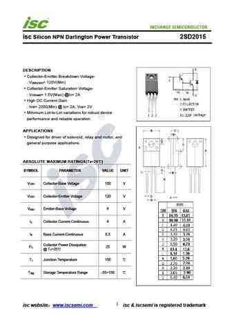
isc Silicon NPN Darlington Power Transistor 2SD2015 DESCRIPTION Collector-Emitter Breakdown Voltage- V = 120V(Min) (BR)CEO Collector-Emitter Saturation Voltage- V = 1.5V(Max) @I = 2A CE(sat) C High DC Current Gain h = 2000(Min) @ I = 2A, V = 2V FE C CE Minimum Lot-to-Lot variations for robust device performance and reliable operation APPLICATIONS Designed for drive
Otros transistores... APM9968C
, APM9968CO
, APM9984CCG
, APM9986CO
, APM9988CO
, APM9988QA
, SIR164DP
, 1481
, IRFB4115
, 2016
, 2021
, 2026
, 2341
, 4401
, 4402
, 4407
, 4409
.