4435 Datasheet. Equivalente. Reemplazo. Hoja de especificaciones. Principales características
Número de Parte: 4435 📄📄
Tipo de FET: MOSFET
Polaridad de transistor: P
ESPECIFICACIONES MÁXIMAS
Pdⓘ - Máxima disipación de potencia: 3.1 W
|Vds|ⓘ - Voltaje máximo drenador-fuente: 30 V
|Vgs|ⓘ - Voltaje máximo fuente-puerta: 20 V
|Id|ⓘ - Corriente continua de drenaje: 8 A
Tjⓘ - Temperatura máxima de unión: 150 °C
CARACTERÍSTICAS ELÉCTRICAS
RDSonⓘ - Resistencia estado encendido drenaje a fuente: 0.02 Ohm
Encapsulados: SOP8
📄📄 Copiar
Búsqueda de reemplazo de 4435 MOSFET
- Selecciónⓘ de transistores por parámetros
4435 datasheet
4435.pdf
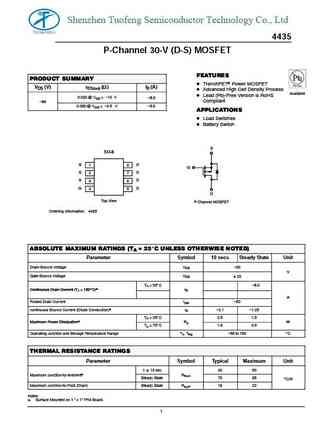
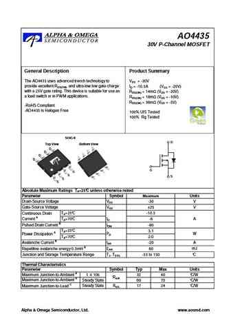
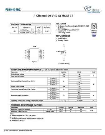
Shenzhen Tuofeng Semiconductor Technology Co., Ltd 4435 P-Channel 30-V (D-S) MOSFET FEATURES PRODUCT SUMMARY D TrenchFETr Power MOSFET VDS (V) rDS(on) (W) ID (A) D Advanced High Cell Density Process Available D Lead (Pb)-Free Version is RoHS 0.020 @ VGS = -10 V -8.0 Compliant -30 -30 0.030 @ VGS = -4.5 V -5.0 APPLICATIONS D Load Switches D Battery Switch S SO-8 SD 1 8 G
4435.pdf
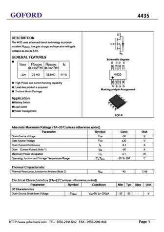
GOFORD 4435 D DESCRIPTION The 4435 uses ad vanced trench technology to provide G excellent RDS(ON), low gate charge and operation with gate voltages as low as 4.5V. S GENERAL FEATURES Schematic diagram VDSS RDS(ON) RDS(ON) ID @ (Typ) @ -4.5V -10V (Typ) m m -30V 21 15.5 -9.1 A High Power and current handing capability Lead free product is acquired M
4435.pdf
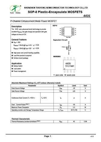
SHENZHEN TUOFENG SEMICONDUCTOR TECHNOLOGY CO.,LTD SOP-8 Plastic-Encapsulate MOSFETS 4435 P-Channel Enhancement Mode Power MOSFET SOP-8 Description SD 1 8 The 4435 uses advanced trench technology to provide S D 2 7 excellent RDS(ON), low gate charge and operation with gate SD 3 6 G D voltages as low as 4.5V. 4 5 Top View General Features Equivalent Cir cuit S VDS =
irf4435.pdf
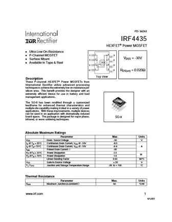
PD- 94243 IRF4435 HEXFET Power MOSFET Ultra Low On-Resistance A 1 8 S D P-Channel MOSFET VDSS = -30V 2 7 Surface Mount S D Available in Tape & Reel 3 6 S D 4 5 G D RDS(on) = 0.020 Top View Description These P-channel HEXFET Power MOSFETs from International Rectifier utilize advanced processing techniques to achieve the extremely low on-resistance per silicon ar
si4435dy.pdf

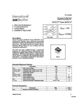
PD- 93768A Si4435DY HEXFET Power MOSFET Ultra Low On-Resistance A 1 8 S D P-Channel MOSFET VDSS = -30V 2 7 Surface Mount S D Available in Tape & Reel 3 6 S D 4 5 G D RDS(on) = 0.020 Top View Description These P-channel HEXFET Power MOSFETs from International Rectifier utilize advanced processing techniques to achieve the extremely low on-resistance per silicon
2sc4435.pdf
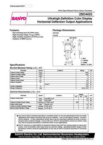
Ordering number EN3791 NPN Triple Diffused Planar Silicon Transistor 2SC4435 Ultrahigh-Definition Color Display Horizontal Deflection Output Applications Features Package Dimensions Fast switching speed (tf=300ns max). unit mm High brocking voltage (VCBO=1500V). 2022A High reliability (Adoption of HVP process). [2SC4435] Adoption of MBIT process. 15.6 3.2 4.8 14.
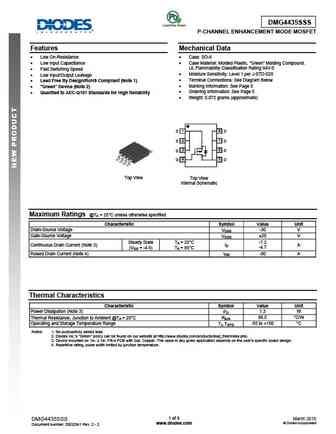
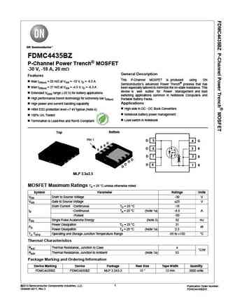
fdmc4435bz.pdf
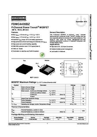
September 2010 FDMC4435BZ P-Channel Power Trench MOSFET -30 V, -18 A, 20 m Features General Description Max rDS(on) = 20 m at VGS = -10 V, ID = -8.5 A This P-Channel MOSFET is produced using Fairchild Semiconductor s advanced Power Trench process that has Max rDS(on) = 37 m at VGS = -4.5 V, ID = -6.3 A been especially tailored to minimize the on-state resistance. This E
fdms4435bz.pdf
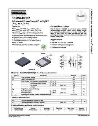
March 2011 FDMS4435BZ P-Channel PowerTrench MOSFET -30 V, -18 A, 20 m Features General Description Max rDS(on) = 20 m at VGS = -10 V, ID = -9.0 A This P-Channel MOSFET is produced using Fairchild Max rDS(on) = 37 m at VGS = -4.5 V, ID = -6.5 A Semiconductor s advanced Power Trench process that has been especially tailored to minimize the on-state resistance. This Exte
fds4435.pdf
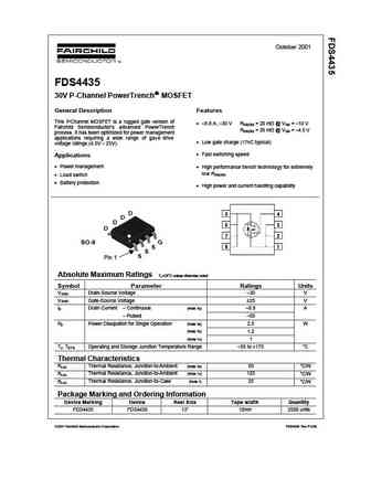
October 2001 FDS4435 30V P-Channel PowerTrench MOSFET General Description Features This P MOSFET is a rugged gate version of -Channel 8.8 A, 30 V R = 20 m @ V = 10 V DS(ON) GS Fairchild Semiconductor s advanced PowerTrench R = 35 m @ V = 4.5 V DS(ON) GS process. It has been optimized for power management applications requiring a wide range of gave
fds4435bz f085.pdf
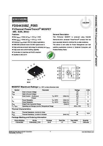
July 2009 FDS4435BZ_F085 P-Channel PowerTrench MOSFET -30V, -8.8A, 20m Features General Description Max rDS(on) = 20m at VGS = -10V, ID = -8.8A This P-Channel MOSFET is produced using Fairchild Max rDS(on) = 35m at VGS = -4.5V, ID = -6.7A Semiconductor s advanced PowerTrench process that has Extended VGSS range (-25V) for battery applications been especially tailored to mi
si4435dy.pdf

October 2001 SI4435DY 30V P-Channel PowerTrench MOSFET General Description Features This P MOSFET is a rugged gate version of -Channel 8.8 A, 30 V R = 20 m @ V = 10 V DS(ON) GS Fairchild Semiconductor s advanced PowerTrench R = 35 m @ V = 4.5 V DS(ON) GS process. It has been optimized for power management applications requiring a wide range of gave
fds4435a.pdf
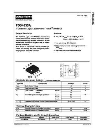
October 2001 FDS4435A P-Channel Logic Level PowerTrench MOSFET General Description Features This P-Channel Logic Level MOSFET is produced using -9 A, -30 V. RDS(ON) = 0.017 W @ VGS = -10 V Fairchild Semiconductor s advanced PowerTrench process RDS(ON) = 0.025 W @ VGS = -4.5 V that has been especially tailored to minimize the on-state resistance and yet maintain low gate charg
fds4435bz.pdf
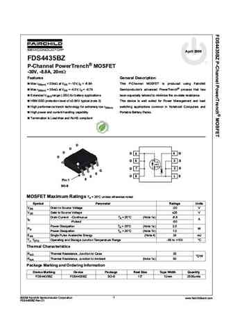
April 2009 FDS4435BZ P-Channel PowerTrench MOSFET -30V, -8.8A, 20m Features General Description Max rDS(on) = 20m at VGS = -10V, ID = -8.8A This P-Channel MOSFET is produced using Fairchild Max rDS(on) = 35m at VGS = -4.5V, ID = -6.7A Semiconductor s advanced PowerTrench process that has Extended VGSS range (-25V) for battery applications been especially tailored to minimi
si4435dytr.pdf
PD- 93768A Si4435DY HEXFET Power MOSFET Ultra Low On-Resistance A 1 8 S D P-Channel MOSFET VDSS = -30V 2 7 Surface Mount S D Available in Tape & Reel 3 6 S D 4 5 G D RDS(on) = 0.020 Top View Description These P-channel HEXFET Power MOSFETs from International Rectifier utilize advanced processing techniques to achieve the extremely low on-resistance per silicon
sq4435ey.pdf
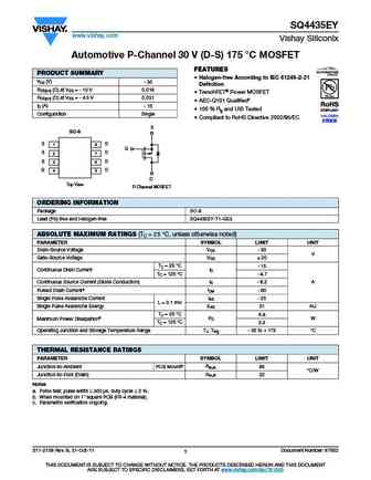
SQ4435EY www.vishay.com Vishay Siliconix Automotive P-Channel 30 V (D-S) 175 C MOSFET FEATURES PRODUCT SUMMARY Halogen-free According to IEC 61249-2-21 VDS (V) - 30 Definition RDS(on) ( ) at VGS = - 10 V 0.018 TrenchFET Power MOSFET RDS(on) ( ) at VGS = - 4.5 V 0.031 AEC-Q101 Qualifiedc ID (A) - 15 100 % Rg and UIS Tested Configuration Single Complian
si4435ddy.pdf
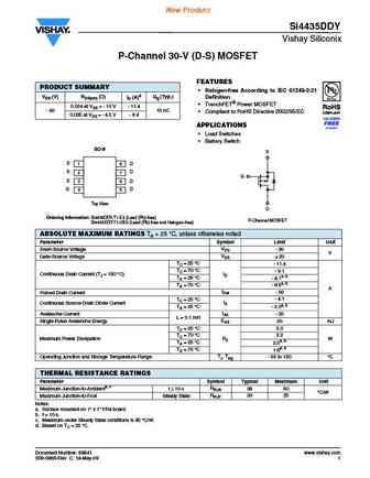
New Product Si4435DDY Vishay Siliconix P-Channel 30-V (D-S) MOSFET FEATURES PRODUCT SUMMARY Halogen-free According to IEC 61249-2-21 VDS (V) RDS(on) ( ) ID (A)d Qg (Typ.) Definition TrenchFET Power MOSFET 0.024 at VGS = - 10 V - 11.4 - 30 15 nC Compliant to RoHS Directive 2002/95/EC 0.035 at VGS = - 4.5 V - 9.4 APPLICATIONS Load Switches Battery Swit
si4435dd.pdf

New Product Si4435DDY Vishay Siliconix P-Channel 30-V (D-S) MOSFET FEATURES PRODUCT SUMMARY Halogen-free According to IEC 61249-2-21 VDS (V) RDS(on) ( ) ID (A)d Qg (Typ.) Definition TrenchFET Power MOSFET 0.024 at VGS = - 10 V - 11.4 - 30 15 nC Compliant to RoHS Directive 2002/95/EC 0.035 at VGS = - 4.5 V - 9.4 APPLICATIONS Load Switches Battery Swit
si4435dy.pdf
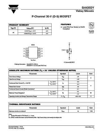
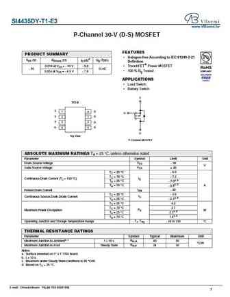
Si4435DY Vishay Siliconix P-Channel 30-V (D-S) MOSFET FEATURES PRODUCT SUMMARY D Lead (Pb)-Free Version is RoHS VDS (V) rDS(on) (W) ID (A) Compliant 0.02 @ VGS = 10 V 8.0 30 30 0.035 @ VGS = 4.5 V 6.0 S SO-8 SD 1 8 G S D 2 7 SD 3 6 G D 4 5 D Top View P-Channel MOSFET Ordering Information Si4435DY-T1 REV A Si4435DY-T1 A E3 (Lead (Pb)-Free) ABSOLU
si4435dypbf si4435dytrpbf.pdf

PD- 95133 Si4435DYPbF HEXFET Power MOSFET l Ultra Low On-Resistance A 1 8 S D l P-Channel MOSFET VDSS = -30V 2 7 l Surface Mount S D l Available in Tape & Reel 3 6 S D l Lead-Free 4 5 G D RDS(on) = 0.020 Top View Description These P-channel HEXFET Power MOSFETs from International Rectifier utilize advanced processing techniques to achieve the extremely low on-resis
si4435fdy.pdf
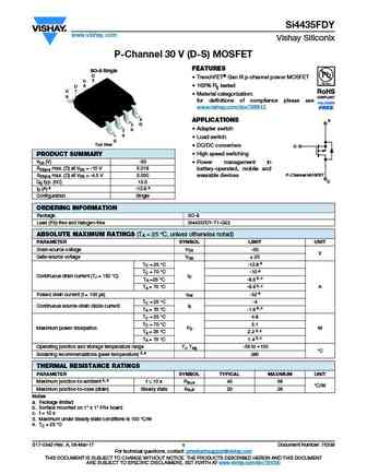
Si4435FDY www.vishay.com Vishay Siliconix P-Channel 30 V (D-S) MOSFET FEATURES SO-8 Single D TrenchFET Gen III p-channel power MOSFET D 5 D 6 100% Rg tested D 7 Material categorization 8 for definitions of compliance please see www.vishay.com/doc?99912 4 APPLICATIONS S G 3 3 Adapter switch S S 2 2 S S 1 1 Load switch S Top View DC
si4435bdy.pdf
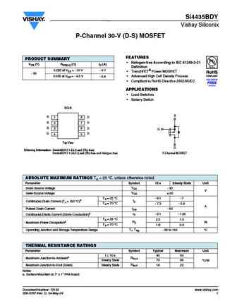
Si4435BDY Vishay Siliconix P-Channel 30-V (D-S) MOSFET FEATURES PRODUCT SUMMARY Halogen-free According to IEC 61249-2-21 VDS (V) RDS(on) ( )ID (A) Definition 0.020 at VGS = - 10 V - 9.1 TrenchFET Power MOSFET - 30 0.035 at VGS = - 4.5 V Advanced High Cell Density Process - 6.9 Compliant to RoHS Directive 2002/95/EC APPLICATIONS Load Switches B
dmg4435sss.pdf
DMG4435SSS P-CHANNEL ENHANCEMENT MODE MOSFET Features Mechanical Data Low On-Resistance Case SO-8 Low Input Capacitance Case Material Molded Plastic, Green Molding Compound. UL Flammability Classification Rating 94V-0 Fast Switching Speed Moisture Sensitivity Level 1 per J-STD-020 Low Input/Output Leakage Terminal Connections See Diagram
si4435dypbf.pdf
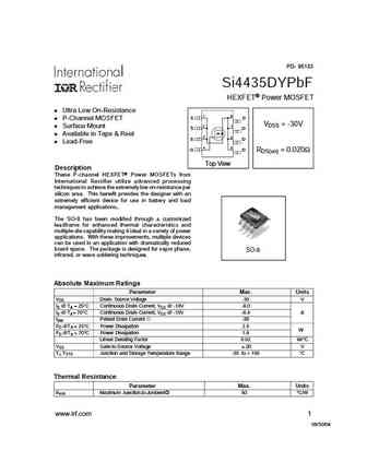
PD- 95133 Si4435DYPbF HEXFET Power MOSFET l Ultra Low On-Resistance A 1 8 S D l P-Channel MOSFET VDSS = -30V 2 7 l Surface Mount S D l Available in Tape & Reel 3 6 S D l Lead-Free 4 5 G D RDS(on) = 0.020 Top View Description These P-channel HEXFET Power MOSFETs from International Rectifier utilize advanced processing techniques to achieve the extremely low on-resis
fdmc4435bz.pdf
FDMC4435BZ P-Channel Power Trench MOSFET -30 V, -18 A, 20 m General Description Features This P-Channel MOSFET is produced using ON Max rDS(on) = 20 m at VGS = -10 V, ID = -8.5 A Semiconductor s advanced Power Trench process that has Max rDS(on) = 37 m at VGS = -4.5 V, ID = -6.3 A been especially tailored to minimize the on-state resistance. This device is well suited
fdms4435bz.pdf

Is Now Part of To learn more about ON Semiconductor, please visit our website at www.onsemi.com Please note As part of the Fairchild Semiconductor integration, some of the Fairchild orderable part numbers will need to change in order to meet ON Semiconductor s system requirements. Since the ON Semiconductor product management systems do not have the ability to manage part nomenclatur
fds4435bz.pdf

Is Now Part of To learn more about ON Semiconductor, please visit our website at www.onsemi.com Please note As part of the Fairchild Semiconductor integration, some of the Fairchild orderable part numbers will need to change in order to meet ON Semiconductor s system requirements. Since the ON Semiconductor product management systems do not have the ability to manage part nomenclatur
ut4435.pdf
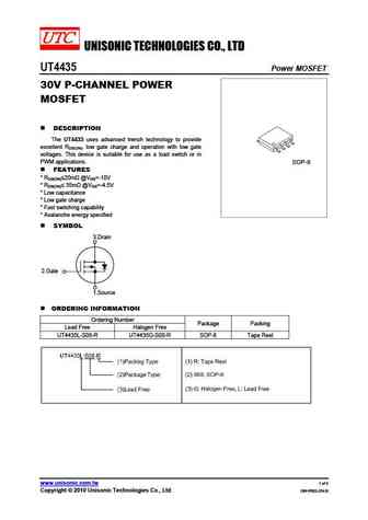
UNISONIC TECHNOLOGIES CO., LTD UT4435 Power MOSFET 30V P-CHANNEL POWER MOSFET DESCRIPTION The UT4435 uses advanced trench technology to provide excellent RDS(ON), low gate charge and operation with low gate voltages. This device is suitable for use as a load switch or in PWM applications. SOP-8 FEATURES * RDS(ON) 20m @VGS=-10V * RDS(ON) 35m @VGS=-4.5V * L
ssg4435.pdf
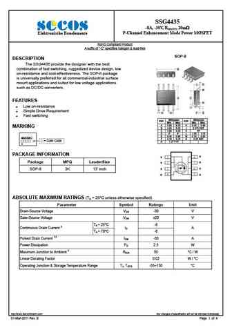
SSG4435 -8A, -30V, RDS(ON) 20m P-Channel Enhancement Mode Power MOSFET Elektronische Bauelemente RoHS Compliant Product A suffix of -C specifies halogen & lead-free SOP-8 DESCRIPTION The SSG4435 provide the designer with the best B combination of fast switching, ruggedized device design, low on-resistance and cost-effectiveness. The SOP-8 package is universal
tsm4435cs.pdf
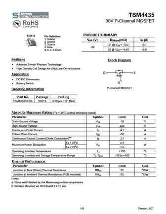
TSM4435 30V P-Channel MOSFET PRODUCT SUMMARY SOP-8 Pin Definition 1. Source VDS (V) RDS(on)(m ) ID (A) 2. Source 3. Source 21 @ VGS = -10V -9.1 4. Gate -30 35 @ VGS = -4.5V -6.9 5, 6, 7, 8. Drain Features Block Diagram Advance Trench Process Technology High Density Cell Design for Ultra Low On-resistance Application DC-DC Conversion Ba
tsm4435bcs.pdf
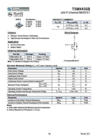
TSM4435B 30V P-Channel MOSFET SOP-8 Pin Definition PRODUCT SUMMARY 1. Source 8. Drain VDS (V) RDS(on)(m ) ID (A) 2. Source 7. Drain 3. Source 6. Drain 21 @ VGS = -10V -9.1 4. Gate 5. Drain -30 35 @ VGS = -4.5V -6.9 Features Block Diagram Advance Trench Process Technology High Density Cell Design for Ultra Low On-resistance Application DC-DC Conv
cjq4435.pdf
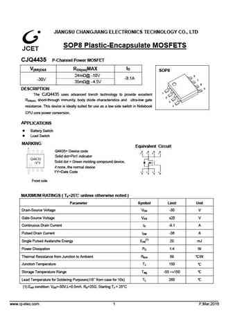
JIANGSU CHANGJIANG ELECTRONICS TECHNOLOGY CO., LTD SOP8 Plastic-Encapsulate MOSFETS CJQ4435 P-Channel Power MOSFET ID V(BR)DSS R DS(on) MAX SOP8 24 -10V m @ -9.1A -30V 35m @ -4.5 V DESCRIPTION The CJQ4435 uses advanced trench technology to provide excellent RDS(on), shoot-through immunity, body diode characteristics and ultra-low gate resistance. This device is idea
cjq4435s.pdf
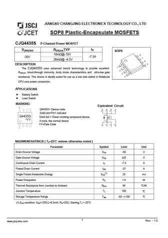
JIANGSU CHANGJING ELECTRONICS TECHNOLOGY CO., LTD SOP8 Plastic-Encapsulate MOSFETS CJQ4435S P-Channel Power MOSFET ID R DS(o n) TYP V(BR)DSS SOP8 18m @-10V -30V -7.3A 26m @ -4.5V DESCRIPTION The CJQ4435S uses advanced trench technology to provide excellent RDS(on), shoot-through immunity, body diode characteristics and ultra-low gate resistance. This device is ideally
cjd4435.pdf
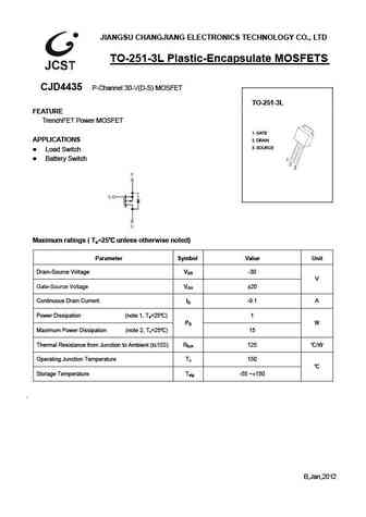
JIANGSU CHANGJIANG ELECTRONICS TECHNOLOGY CO., LTD TO-251-3L Plastic-Encapsulate MOSFETS CJD4435 P-Channel 30-V(D-S) MOSFET TO-251-3L FEATURE TrenchFET Power MOSFET 1. GATE APPLICATIONS 2. DRAIN 3. SOURCE Load Switch Battery Switch Maximum ratings ( Ta=25 unless otherwise noted) Parameter Symbol Value Unit Drain-Source Voltage VDS -30 V Gate-Source Voltage
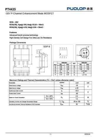
pt4435.pdf
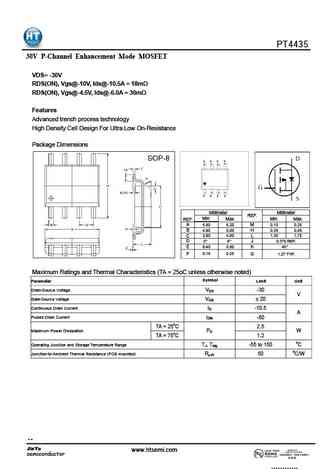
PT4435 30V P-Channel Enhancement Mode MOSFET VDS= -30V RDS(ON), Vgs@-10V, Ids@-10.5A = 18m RDS(ON), Vgs@-4.5V, Ids@-6.0A = 30m Features Advanced trench process technology High Density Cell Design For Ultra Low On-Resistance Package Dimensions D D D D 8 7 6 5 1 2 3 4 S S S G Millimeter Millimeter REF. Min. Max. Min. Max. REF. A 5.80 6.20 M 0.10 0.25 B 4.80
cet4435a.pdf
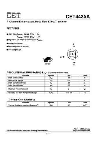
CET4435A P-Channel Enhancement Mode Field Effect Transistor FEATURES -30V, -8.8A, RDS(ON) = 24m @VGS = -10V. RDS(ON) = 35m @VGS = -4.5V. High dense cell design for extremely low RDS(ON). Rugged and reliable. D Lead free product is acquired. SOT-223 package. G D S D G SOT-223 S ABSOLUTE MAXIMUM RATINGS TA = 25 C unless otherwise noted Parameter Symbol Limit Units Drain-
cem4435a.pdf
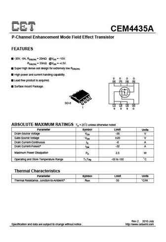
CEM4435A P-Channel Enhancement Mode Field Effect Transistor FEATURES -30V, -8A, RDS(ON) = 20m @VGS = -10V. RDS(ON) = 33m @VGS = -4.5V. Super high dense cell design for extremely low RDS(ON). High power and current handing capability. D D D D Lead free product is acquired. 8 7 6 5 Surface mount Package. SO-8 1 2 3 4 1 S S S G ABSOLUTE MAXIMUM RATINGS TA = 25 C unless other
wtk4435.pdf
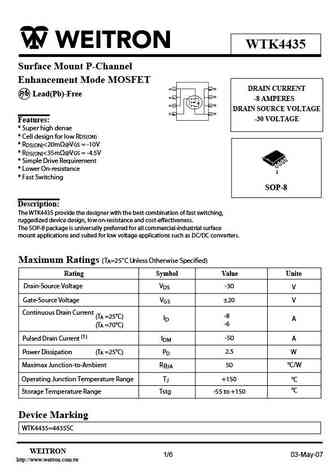
WTK4435 Surface Mount P-Channel Enhancement Mode MOSFET DRAIN CURRENT P b Lead(Pb)-Free -8 AMPERES DRAIN SOURCE VOLTAGE -30 VOLTAGE Features * Super high dense * Cell design for low RDS(ON) * R
h4435s.pdf
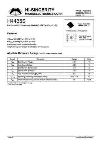
Spec. No. MOS200101) HI-SINCERITY Issued Date 2008.01.12 Revised Date 2009.02.06 MICROELECTRONICS CORP. Page No. 1/5 H4435S 8-Lead Plastic SO-8 Package Code S P-Channel Enhancement-Mode MOSFET (-30V, -9.1A) H4435S Symbol & Pin Assignment Features 5 4 Pin 1 / 2 / 3 Source 6 3 Pin 4 Gate 7 2 RDS(on)=20m @VGS=-10V, ID=-9.1A Pin 5 / 6 / 7 / 8 Dr
ao4435.pdf
AO4435 30V P-Channel MOSFET General Description Product Summary The AO4435 uses advanced trench technology to VDS = -30V provide excellent RDS(ON), and ultra-low low gate charge ID = -10.5A (VGS = -20V) with a 25V gate rating. This device is suitable for use as RDS(ON)
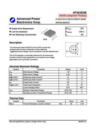
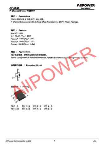
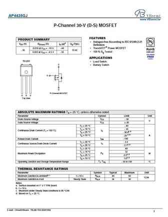
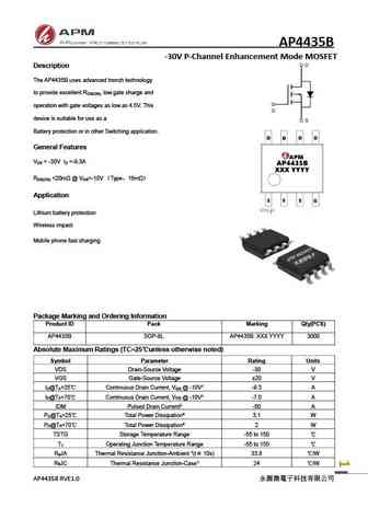
ap4435gm-hf.pdf
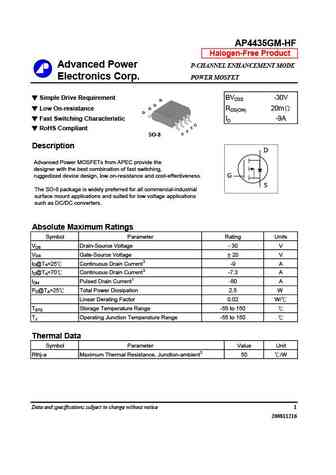
AP4435GM-HF Halogen-Free Product Advanced Power P-CHANNEL ENHANCEMENT MODE Electronics Corp. POWER MOSFET Simple Drive Requirement BVDSS -30V D D D Low On-resistance RDS(ON) 20m D Fast Switching Characteristic ID -9A G S RoHS Compliant S S SO-8 Description D Advanced Power MOSFETs from APEC provide the designer with the best combination of fast switching,
ap4435gh ap4435gj.pdf
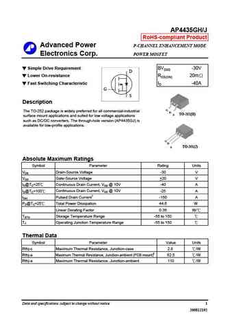
AP4435GH/J RoHS-compliant Product Advanced Power P-CHANNEL ENHANCEMENT MODE Electronics Corp. POWER MOSFET Simple Drive Requirement BVDSS -30V D Lower On-resistance RDS(ON) 20m Fast Switching Characteristic ID -40A G S Description G The TO-252 package is widely preferred for all commercial-industrial D S TO-252(H) surface mount applications and suited for low voltag
ap4435gh-hf ap4435gj-hf.pdf
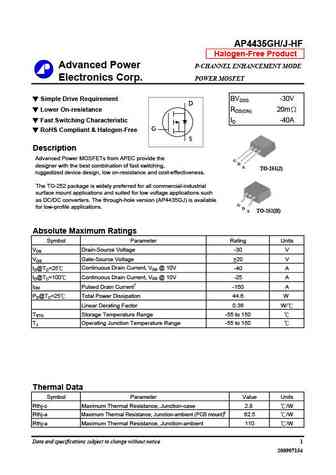
AP4435GH/J-HF Halogen-Free Product Advanced Power P-CHANNEL ENHANCEMENT MODE Electronics Corp. POWER MOSFET Simple Drive Requirement BVDSS -30V D Lower On-resistance RDS(ON) 20m Fast Switching Characteristic ID -40A G RoHS Compliant & Halogen-Free S Description Advanced Power MOSFETs from APEC provide the G D designer with the best combination of fast switching,
ap4435gm.pdf
AP4435GM RoHS-compliant Product Advanced Power P-CHANNEL ENHANCEMENT MODE Electronics Corp. POWER MOSFET Simple Drive Requirement BVDSS -30V D D Low On-resistance D RDS(ON) 20m D Fast Switching Characteristic ID -9A G S S SO-8 S Description D The Advanced Power MOSFETs from APEC provide the designer with the best combination of fast switching, ruggedized device d
ap4435gyt-hf.pdf
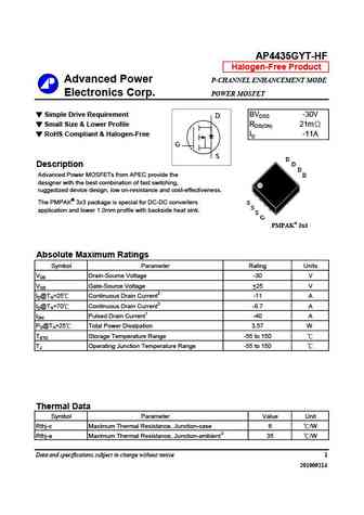
AP4435GYT-HF Halogen-Free Product Advanced Power P-CHANNEL ENHANCEMENT MODE Electronics Corp. POWER MOSFET Simple Drive Requirement BVDSS -30V D Small Size & Lower Profile RDS(ON) 21m RoHS Compliant & Halogen-Free ID -11A G S D D Description D Advanced Power MOSFETs from APEC provide the D designer with the best combination of fast switching, ruggedized device des
afp4435s.pdf
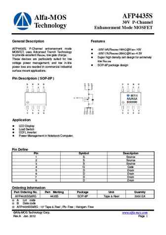
AFP4435S Alfa-MOS 30V P-Channel Technology Enhancement Mode MOSFET General Description Features AFP4435S, P-Channel enhancement mode -30V/-9A,RDS(ON)=18m @VGS=-10V MOSFET, uses Advanced Trench Technology -30V/-7A,RDS(ON)=26m @VGS=-4.5V to provide excellent RDS(ON), low gate charge. Super high density cell design for extremely These devices are particularly suited
afp4435.pdf

AFP4435 Alfa-MOS 30V P-Channel Technology Enhancement Mode MOSFET General Description Features AFP4435, P-Channel enhancement mode -30V/-10A,RDS(ON)=28m @VGS=-10V MOSFET, uses Advanced Trench Technology -30V/ - 7A,RDS(ON)=45m @VGS=-4.5V to provide excellent RDS(ON), low gate charge. Super high density cell design for extremely These devices are particularly suited
afp4435ws.pdf
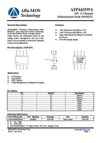
AFP4435WS Alfa-MOS 30V P-Channel Technology Enhancement Mode MOSFET General Description Features AFP4435WS, P-Channel enhancement mode -30V/-9A,RDS(ON)=18m @VGS=-10V MOSFET, uses Advanced Trench Technology -30V/-7A,RDS(ON)=26m @VGS=-4.5V to provide excellent RDS(ON), low gate charge. Super high density cell design for extremely These devices are particularly suite
afp4435w.pdf
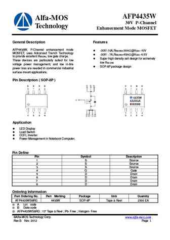
AFP4435W Alfa-MOS 30V P-Channel Technology Enhancement Mode MOSFET General Description Features AFP4435W, P-Channel enhancement mode -30V/-10A,RDS(ON)=30m @VGS=-10V MOSFET, uses Advanced Trench Technology -30V/ - 7A,RDS(ON)=45m @VGS=-4.5V to provide excellent RDS(ON), low gate charge. Super high density cell design for extremely These devices are particularly suit
mtp4435v8.pdf
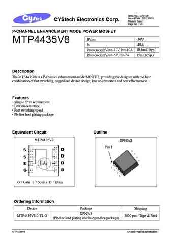
Spec. No. C391V8 Issued Date 2012.09.28 CYStech Electronics Corp. Revised Date Page No. 1/9 P-CHANNEL ENHANCEMENT MODE POWER MOSFET BVDSS -30V MTP4435V8 ID -40A 10.3m (typ.) RDSON(MAX)@VGS=-10V, ID=-10A 15m (typ.) RDSON(MAX)@VGS=-5V, ID=-7A Description The MTP4435V8 is a P-channel enhancement-mode MOSFET, providing the designer with the best combination of
mtp4435aq8.pdf
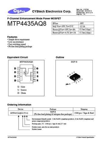
Spec. No. C107Q8 Issued Date 2015.08.14 CYStech Electronics Corp. Revised Date 2015.12.15 Page No. 1/9 P-Channel Enhancement Mode Power MOSFET BVDSS -30V MTP4435AQ8 ID@ VGS=-10V, TA=25 C -12.3A 12.3m (typ.) RDSON @VGS=-10V, ID=-8A 17.5m (typ.) RDSON @VGS=-4.5V, ID=-5A Features Simple drive requirement Low on-resistance Fast switching speed
mep4435q8.pdf
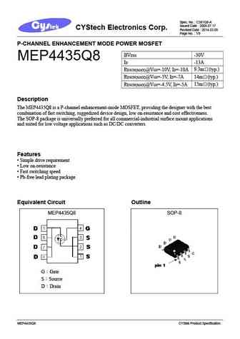
Spec. No. C391Q8-A Issued Date 2008.07.17 CYStech Electronics Corp. Revised Date 2014.03.05 Page No. 1/9 P-CHANNEL ENHANCEMENT MODE POWER MOSFET BVDSS -30V MEP4435Q8 ID -13A 9.3m (typ.) RDSON(MAX)@VGS=-10V, ID=-10A 14m (typ.) RDSON(MAX)@VGS=-5V, ID=-7A 15m (typ.) RDSON(MAX)@VGS=-4.5V, ID=-5A Description The MEP4435Q8 is a P-channel enhancement-mode MOSFE
apm4435k.pdf
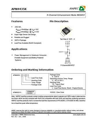
APM4435K P-Channel Enhancement Mode MOSFET Features Pin Description -30V/-8A , RDS(ON)=16m (typ.) @ VGS=-10V RDS(ON)=24m (typ.) @ VGS=-4.5V Super High Dense Cell Design Reliable and Rugged Top View of SOP - 8 SOP-8 Package (1, 2, 3) S S S Lead Free Available (RoHS Compliant) Applications (4)G Power Management in Notebook Computer, Portable Equipment and Batte
stm4435.pdf
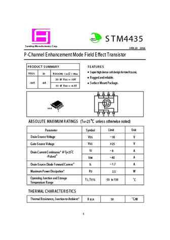
Green Product S TM4435 S amHop Microelectronics C orp. J AN.20 2006 P-Channel E nhancement Mode Field E ffect Transistor PR ODUC T S UMMAR Y F E ATUR E S S uper high dense cell design for low R DS (ON). VDS S ID R DS (ON) ( m ) Max R ugged and reliable. 20 @ VG S = -10V -30V -8A S urface Mount Package. 33 @ VG S = -4.5V D D D D 8 7 6 5 S O-8 1 1 2 3 4 S S S G ABS OLUTE M
brcs4435sc.pdf
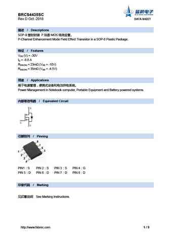
BRCS4435SC Rev.D Oct.-2018 DATA SHEET / Descriptions SOP-8 P MOS P-Channel Enhancement Mode Field Effect Transistor in a SOP-8 Plastic Package. / Features VDS (V) = -30V ID = -8.8 A RDS(ON)
ftk4435.pdf
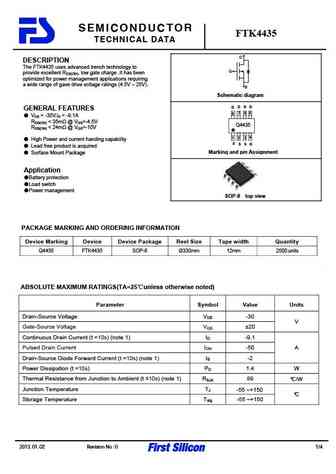
SEMICONDUCTOR FTK4435 TECHNICAL DATA D DESCRIPTION The FTK4435 uses advanced trench technology to G provide excellent RDS(ON), low gate charge .It has been optimized for power management applications requiring a wide range of gave drive voltage ratings (4.5V 25V). S Schematic diagram D D D D GENERAL FEATURES 7 6 5 8 VDS = -30V,ID = -9.1A RDS(ON)
si4435dy.pdf

SMD Type MOSFET SMD Type P-Channel MOSFET SI4435DY (KI4435DY) SOP-8 Features VDS=-30V RDS(on)=0.02 @VGS=-10V 1.50 0.15 RDS(on)=0.035 @VGS=-4.5V S S D 1 8 G S D 2 7 S D 3 6 G D 4 5 D Top View Absolute Maximum Ratings Ta = 25 Parameter Symbol Rating Unit Drain-Source Voltage VDS -30 V Gate-Source Voltage VGS 20 V Continuous Drain Current ID
ao4435.pdf
SMD Type MOSFET P-Channel MOSFET AO4435 (KO4435) SOP-8 Features VDS (V) =-30V ID =-10.5 A (VGS =-20V) 1.50 0.15 RDS(ON) 14m (VGS =-20V) RDS(ON) 18m (VGS =-10V) 1 Source 5 Drain RDS(ON) 36m (VGS =-5V) 6 Drain 2 Source 7 Drain 3 Source 8 Drain 4 Gate D G S Absolute Maximum Ratings Ta = 25 Parameter Symbol Rating Unit Dr
si4435dy ki4435dy.pdf
SMD Type MOSFET SMD Type P-Channel MOSFET SI4435DY (KI4435DY) SOP-8 Features VDS=-30V RDS(on)=0.02 @VGS=-10V 1.50 0.15 RDS(on)=0.035 @VGS=-4.5V S S D 1 8 G S D 2 7 S D 3 6 G D 4 5 D Top View Absolute Maximum Ratings Ta = 25 Parameter Symbol Rating Unit Drain-Source Voltage VDS -30 V Gate-Source Voltage VGS 20 V Continuous Drain Current ID
am4435.pdf
AiT Semiconductor Inc. AM4435 www.ait-ic.com MOSFET -30V P-CHANNEL ENHANCEMENT MODE DESCRIPTION FEATURES The AM4435 is the P-Channel logic enhancement -30V/-8.0A, R =16m (typ)@V =-10V DS(ON) GS mode power field effect transistor is produced -30V/-5.0A, R =26m (typ)@V =-4.5V DS(ON) GS using high cell density. Advanced trench Super high density cell design for extremel
blm4435.pdf
Pb Free Product BLM4435 P-Channel Enhancement Mode Power MOSFET D DESCRIPTION G The BLM4435 uses advanced trench technology to provide excellent R , low gate charge and operation with gate DS(ON) S voltages as low as 4.5V. Schematic diagram GENERAL FEATURES V = -30V,I = -10A DS D R
chm4435ajgp.pdf
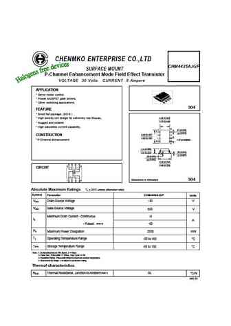
CHENMKO ENTERPRISE CO.,LTD CHM4435AJGP SURFACE MOUNT P-Channel Enhancement Mode Field Effect Transistor VOLTAGE 30 Volts CURRENT 8 Ampere APPLICATION * Servo motor control. * Power MOSFET gate drivers. * Other switching applications. SO-8 FEATURE * Small flat package. (SO-8 ) ( ) * High density cell design for extremely low RDS(ON). 4.06 0.160 ( ) 3.70 0.146 * Rugged and reli
chm4435bjgp.pdf
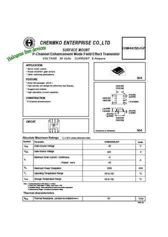
CHENMKO ENTERPRISE CO.,LTD CHM4435BJGP SURFACE MOUNT P-Channel Enhancement Mode Field Effect Transistor VOLTAGE 30 Volts CURRENT 9 Ampere APPLICATION * Servo motor control. * Power MOSFET gate drivers. * Other switching applications. SO-8 FEATURE * Small flat package. (SO-8 ) ( ) * High density cell design for extremely low RDS(ON). 4.06 0.160 ( ) 3.70 0.146 * Rugged and reli
chm4435azgp.pdf
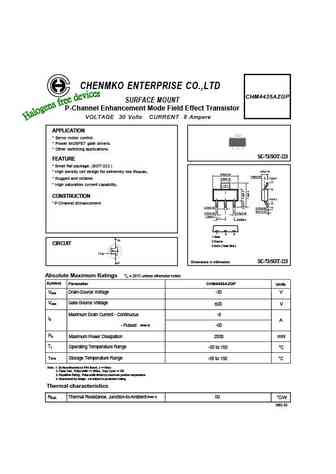
CHENMKO ENTERPRISE CO.,LTD CHM4435AZGP SURFACE MOUNT P-Channel Enhancement Mode Field Effect Transistor VOLTAGE 30 Volts CURRENT 8 Ampere APPLICATION * Servo motor control. * Power MOSFET gate drivers. * Other switching applications. SC-73/SOT-223 FEATURE * Small flat package. (SOT-223 ) 1.65+0.15 * High density cell design for extremely low RDS(ON). 6.50+0.20 0.90+0.05 2.0+
gsm4435ws.pdf
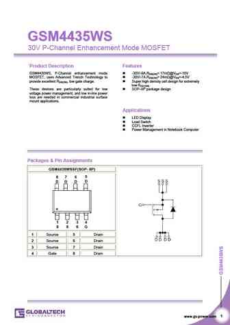
GSM4435WS GSM4435WS 30V P-Channel Enhancement Mode MOSFET Product Description Features GSM4435WS, P-Channel enhancement mode -30V/-9A,RDS(ON)= 17m @VGS=-10V MOSFET, uses Advanced Trench Technology to -30V/-7A,RDS(ON)= 24m @VGS=-4.5V provide excellent RDS(ON), low gate charge. Super high density cell design for extremely low RDS (ON) These devices are particularly suited
gsm4435w.pdf
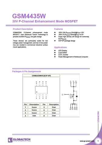
GSM4435W 30V P-Channel Enhancement Mode MOSFET Product Description Features GSM4435W, P-Channel enhancement mode -30V/-10A,RDS(ON)=24m @VGS=-10V MOSFET, uses Advanced Trench Technology to -30V/-7A,RDS(ON)=35m @VGS=-4.5V provide excellent RDS(ON), low gate charge. Super high density cell design for extremely low RDS (ON) These devices are particularly suited for low SOP-
gsm4435.pdf
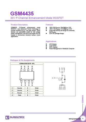
GSM4435 GSM4435 30V P-Channel Enhancement Mode MOSFET Product Description Features GSM4435, P-Channel enhancement mode -30V/-10A,RDS(ON)= 28m @VGS=-10V MOSFET, uses Advanced Trench Technology to -30V/-7.0A,RDS(ON)= 37m @VGS=-4.5V provide excellent RDS(ON), low gate charge. These Super high density cell design for extremely devices are particularly suited for low voltage lo
gsm4435s.pdf
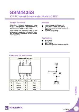
GSM4435S GSM4435S 30V P-Channel Enhancement Mode MOSFET Product Description Features GSM4435S, P-Channel enhancement mode -30V/-9A,RDS(ON)=18m @VGS=-10V MOSFET, uses Advanced Trench Technology to -30V/-7A,RDS(ON)=26m @VGS=-4.5V provide excellent RDS(ON), low gate charge. Super high density cell design for extremely low RDS (ON) These devices are particularly suited for
me4435 me4435-g.pdf
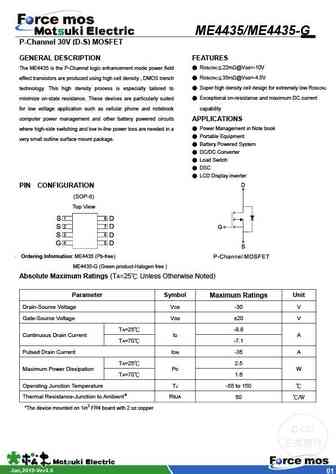
ME4435/ME4435-G P-Channel 30V (D-S) MOSFET GENERAL DESCRIPTION FEATURES The ME4435 is the P-Channel logic enhancement mode power field RDS(ON) 22m @VGS=-10V effect transistors are produced using high cell density , DMOS trench RDS(ON) 35m @VGS=-4.5V technology. This high density process is especially tailored to Super high density cell design for extremely low RDS(ON)
mmp4435bdy.pdf
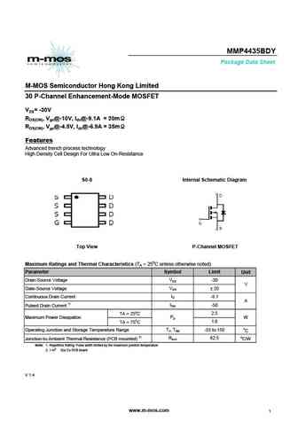
MMP4435BDY Package Data Sheet M-MOS Semiconductor Hong Kong Limited 30 P-Channel Enhancement-Mode MOSFET VDS= -30V RDS(ON), Vgs@-10V, Ids@-9.1A = 20m RDS(ON), Vgs@-4.5V, Ids@-6.9A = 35m Features Advanced trench process technology High Density Cell Design For Ultra Low On-Resistance S0-8 Internal Schematic Diagram Top View P-Channel MOSFET Maximum Ratings and Thermal Characteri
nce4435.pdf
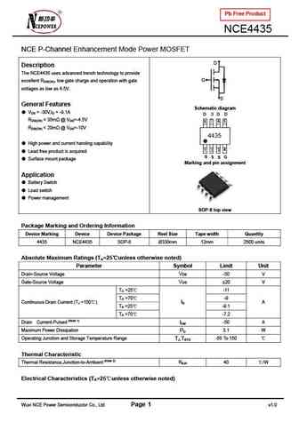
Pb Free Product NCE4435 NCE P-Channel Enhancement Mode Power MOSFET D Description The NCE4435 uses advanced trench technology to provide G excellent RDS(ON), low gate charge and operation with gate voltages as low as 4.5V. S General Features Schematic diagram VDS = -30V,ID = -9.1A RDS(ON)
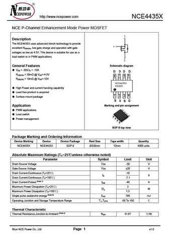
nce4435b.pdf
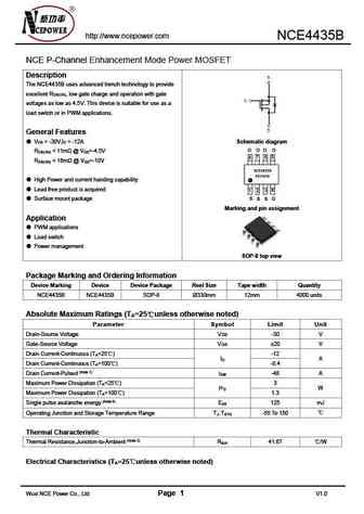
http //www.ncepower.com NCE4435B NCE P-Channel Enhancement Mode Power MOSFET Description The NCE4435B uses advanced trench technology to provide excellent R , low gate charge and operation with gate DS(ON) voltages as low as 4.5V. This device is suitable for use as a load switch or in PWM applications. General Features V = -30V,I = -12A Schematic diagram DS D R
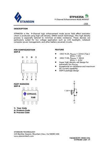
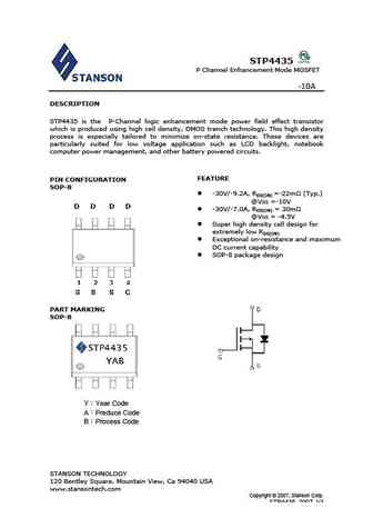
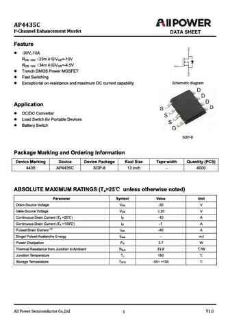
stp4435.pdf
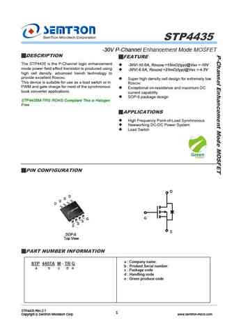
STP4435 -30V P-Channel Enhancement Mode MOSFET DESCRIPTION FEATURE The STP4435 is the P-Channel logic enhancement -30V/-10.0A, RDS(ON) =15m (typ)@VGS =-10V mode power field effect transistor is produced using -30V/-6.0A, RDS(ON) =25m (typ)@VGS =-4.5V high cell density. advanced trench technology to provide excellent RDS(ON). Super high density cell design
ssm4435m.pdf
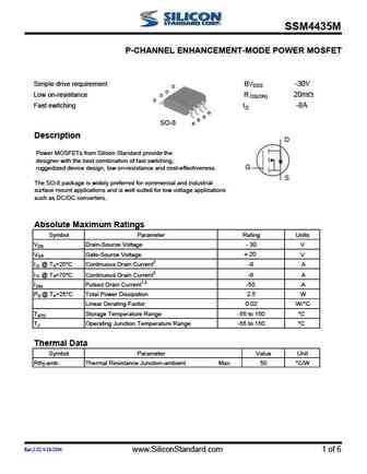
SSM4435M P-CHANNEL ENHANCEMENT-MODE POWER MOSFET Simple drive requirement BVDSS -30V D D Low on-resistance D R 20m DS(ON) D Fast switching ID -8A G S S SO-8 S Description D Power MOSFETs from Silicon Standard provide the designer with the best combination of fast switching, G ruggedized device design, low on-resistance and cost-effectiveness. S The SO-8 package is widely
sl4435a.pdf
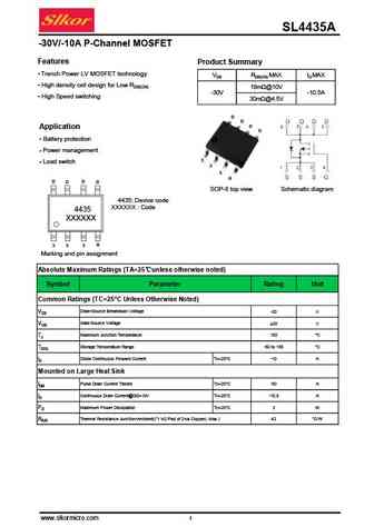
SL4435A -30V/-10A P-Channel MOSFET Features Product Summary Trench Power LV MOSFET technology VDS RDS(ON) MAX ID MAX High density cell design for Low RDS(ON) 18m @10VD2 S1 -30V -10.5A High Speed switching D1 30m @4.5V D D D Application D Battery protection Power management S Load switch S S G D D D D SOP-8 top view Schematic diagram 4435 Dev
stp4435a.pdf
STP4435A P Channel Enhancement Mode MOSFET -10A DESCRIPTION STP4435A is the P-Channel logic enhancement mode power field effect transistor which is produced using high cell density, DMOS trench technology. This high density process is especially tailored to minimize on-state resistance. These devices are particularly suited for low voltage application such as LCD backlight, note
stp4435.pdf
STP4435 P Channel Enhancement Mode MOSFET -10A DESCRIPTION STP4435 is the P-Channel logic enhancement mode power field effect transistor which is produced using high cell density, DMOS trench technology. This high density process is especially tailored to minimize on-state resistance. These devices are particularly suited for low voltage application such as LCD backlight, notebo
as4435s.pdf
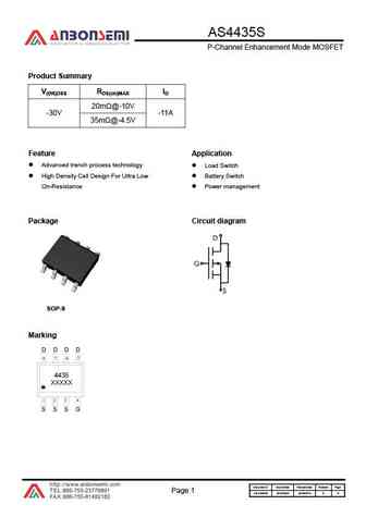
AS4435S P-Channel Enhancement Mode MOSFET Product Summary V(BR)DSS RDS(on)MAX ID 20m @-10V -30V -11A 35m @-4.5V Feature Application Advanced trench process technology Load Switch High Density Cell Design For Ultra Low Battery Switch On-Resistance Power management Package Circuit diagram SOP-8 Marking D D D D 4435 XXXXX S S S G Document ID Issued Date Revi
et4435.pdf
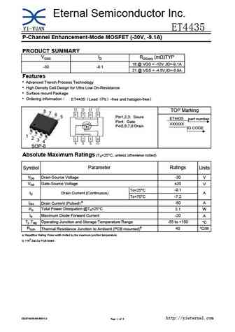
Eternal Semiconductor Inc. ET4435 P-Channel Enhancement-Mode MOSFET (-30V, -9.1A) PRODUCT SUMMARY VDSS ID RDS(on) (m )TYP 16 @ VGS = -10V ,ID=-9.1A -30 -9.1 21 @ VGS = -4.5V,ID=-6.9A Features Advanced Trench Process Technology High Density Cell Design for Ultra Low On-Resistance Surface mount Package Ordering information ET4435 Lead Pb -free and halogen-f
hsm4435.pdf
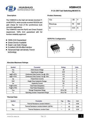
HSM4435 P-Ch 30V Fast Switching MOSFETs Description Product Summary VDS -30 V The HSM4435 is the high cell density trenched P- ch MOSFETs, which provide excellent RDSON and RDS(ON),typ 18 m gate charge for most of the synchronous buck converter applications. ID -9.5 A The HSM4435 meet the RoHS and Green Product requirement, 100% EAS guaranteed with full function reli
jmtp4435a.pdf
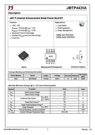
JMTP4435A Description JMT P-channel Enhancement Mode Power MosFET Features Applications -30V, -10A Load Switch RDS(ON)
jst4435.pdf
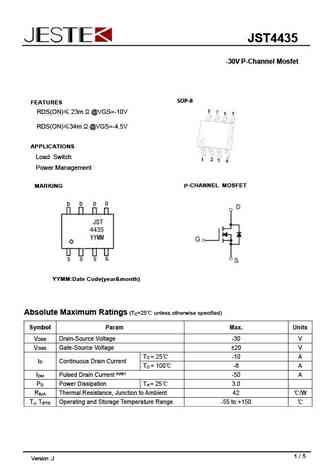
JST4435 -30V P-Channel Mosfet SOP-8 FEATURES RDS(ON) 23m @VGS=-10V RDS(ON) 34m @VGS=-4.5V APPLICATIONS Load Switch Power Management MARKING P-CHANNEL MOSFET YYMM Date Code(year&month) Absolute Maximum Ratings (T =25 unless otherwise specified) C Symbol Param Max. Units bol V Drain-Source Voltage -30 V DSS V Gate-Source Voltage 20 V GSS T = 25 -10 A C I
pt4435.pdf
PT4435 -30V P-Channel Enhancement Mode MOSFET VDS= -30V RDS(ON), Vgs@-10V, Ids@-10.5A = 18m RDS(ON), Vgs@-4.5V, Ids@-6.0A = 30m Features Advanced trench process technology High Density Cell Design For Ultra Low On-Resistance Package Dimensions D D D D 8 7 6 5 1 2 3 S S S G Millimeter Millimeter REF. Min. Max. Min. Max. REF. A 5.80 6.20 M 0.10 0.25 B 4.80
wsp4435a.pdf
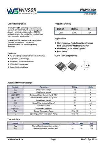
WSP4435A P-Ch MOSFET General Description Product Summery The WSP4435A is the highest performance BVDSS RDSON ID trench P-Ch MOSFET with extreme high cell density , which provide excellent RDSON 20m -30V -8A and gate charge for most of the synchronous buck converter applications . Applications The WSP4435A meet the RoHS and Green Product requirement , 100% EAS High Fre
wsp4435.pdf
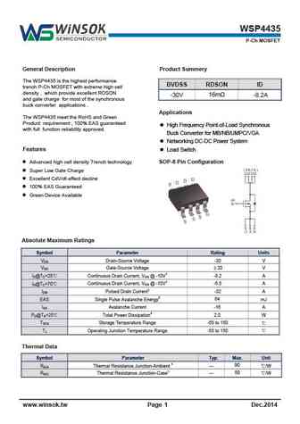
WSP4435 P-Ch MOSFET General Description Product Summery The WSP4435 is the highest performance BVDSS RDSON ID trench P-Ch MOSFET with extreme high cell density , which provide excellent RDSON 16m -30V -8.2A and gate charge for most of the synchronous buck converter applications . Applications The WSP4435 meet the RoHS and Green Product requirement , 100% EAS guaranteed
se4435.pdf
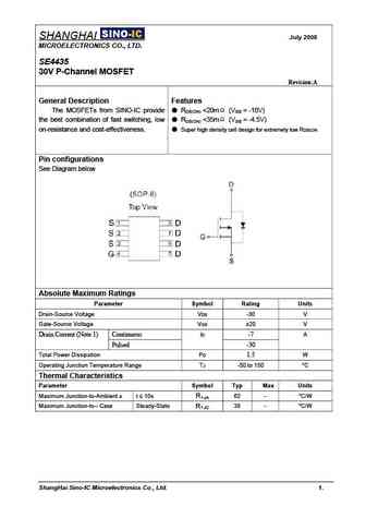
SHANGHAI July 2008 MICROELECTRONICS CO., LTD. SE4435 30V P-Channel MOSFET Revision A General Description Features The MOSFETs from SINO-IC provide RDS(ON)
sm4435.pdf
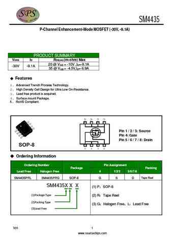
SM4435 P-Channel Enhancement-Mode MOSFET (-30V, -9.1A) PRODUCT SUMMARY VDSS ID RDS(on) (m-ohm) Max 20 @ VGS = -10V ,ID=-9.1A -30V -9.1A 35 @ VGS = -4.5V,ID=-6.9A Features 1 Advanced Trench Process Technology. 2 High Density Cell Design for Ultra Low On-Resistance. Lead free product is acquired 3 . 4 Surface mount Package. 5 RoHS Compliant. Pin 1 / 2 / 3
mt4435actr.pdf

MT4435ACTR www.VBsemi.tw P-Channel 30-V (D-S) MOSFET FEATURES PRODUCT SUMMARY Halogen-free According to IEC 61249-2-21 VDS (V) RDS(on) ( ) ID (A)d Qg (Typ.) Definition 0.018 at VGS = - 10 V - 9.0 TrenchFET Power MOSFET - 30 13 nC 100 % Rg Tested 0.024 at VGS = - 4.5 V - 7.8 APPLICATIONS Load Switch Battery Switch S SO-8 S 1 8 D G S D 2 7 S 3 6 D
fds4435-nl.pdf
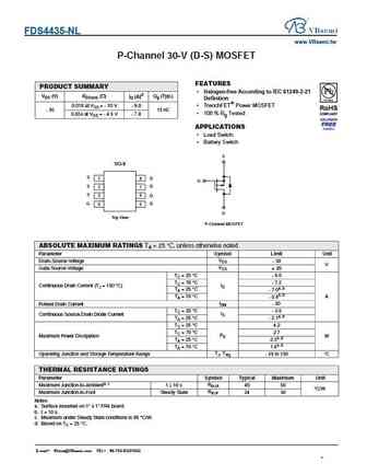
FDS4435-NL www.VBsemi.tw P-Channel 30-V (D-S) MOSFET FEATURES PRODUCT SUMMARY Halogen-free According to IEC 61249-2-21 VDS (V) RDS(on) ( ) ID (A)d Qg (Typ.) Definition 0.018 at VGS = - 10 V - 9.0 TrenchFET Power MOSFET - 30 13 nC 100 % Rg Tested 0.024 at VGS = - 4.5 V - 7.8 APPLICATIONS Load Switch Battery Switch S SO-8 S 1 8 D G S D 2 7 S 3 6 D
vbza4435.pdf
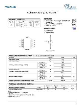
VBZA4435 www.VBsemi.com P-Channel 30-V (D-S) MOSFET FEATURES PRODUCT SUMMARY Halogen-free According to IEC 61249-2-21 VDS (V) RDS(on) ( ) ID (A)d Qg (Typ.) Definition 0.018 at VGS = - 10 V - 9.0 TrenchFET Power MOSFET - 30 13 nC 100 % Rg Tested 0.024 at VGS = - 4.5 V - 7.8 APPLICATIONS Load Switch Battery Switch S SO-8 S 1 8 D G S D 2 7 S 3 6 D
ap4435gj.pdf
AP4435GJ www.VBsemi.tw P-Channel 30-V (D-S) MOSFET FEATURES PRODUCT SUMMARY Halogen-free According to IEC 61249-2-21 VDS (V) RDS(on) ( ) ID (A)d Qg (Typ.) Definition 0.018 at VGS = - 10 V - 40 TrenchFET Power MOSFET - 30 13 nC 100 % Rg Tested 0.022 at VGS = - 4.5 V - 35 APPLICATIONS TO-251 Load Switch S Battery Switch G D P-Channel MOSFET G D S Top
sq4435ey.pdf

SQ4435EY www.VBsemi.tw P-Channel 30-V (D-S) MOSFET FEATURES PRODUCT SUMMARY Halogen-free According to IEC 61249-2-21 VDS (V) RDS(on) ( ) ID (A)d Qg (Typ.) Definition 0.018 at VGS = - 10 V - 9.0 TrenchFET Power MOSFET - 30 13 nC 100 % Rg Tested 0.024 at VGS = - 4.5 V - 7.8 APPLICATIONS Load Switch Battery Switch S SO-8 S 1 8 D G S D 2 7 S 3 6 D
im4435g.pdf
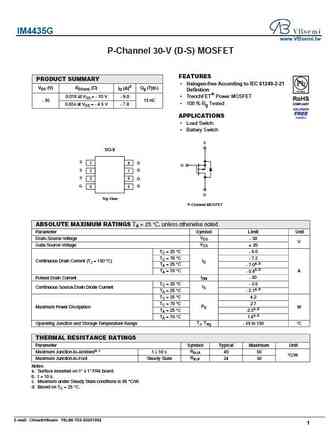
IM4435G www.VBsemi.tw P-Channel 30-V (D-S) MOSFET FEATURES PRODUCT SUMMARY Halogen-free According to IEC 61249-2-21 VDS (V) RDS(on) ( ) ID (A)d Qg (Typ.) Definition 0.018 at VGS = - 10 V - 9.0 TrenchFET Power MOSFET - 30 13 nC 100 % Rg Tested 0.024 at VGS = - 4.5 V - 7.8 APPLICATIONS Load Switch Battery Switch S SO-8 S 1 8 D G S D 2 7 S 3 6 D G
fds4435a.pdf

FDS4435A www.VBsemi.tw P-Channel 30-V (D-S) MOSFET FEATURES PRODUCT SUMMARY Halogen-free According to IEC 61249-2-21 VDS (V) RDS(on) ( ) ID (A)d Qg (Typ.) Definition 0.018 at VGS = - 10 V - 9.0 TrenchFET Power MOSFET - 30 13 nC 100 % Rg Tested 0.024 at VGS = - 4.5 V - 7.8 APPLICATIONS Load Switch Battery Switch S SO-8 S 1 8 D G S D 2 7 S 3 6 D
gf4435.pdf
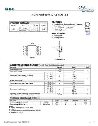
GF4435 www.VBsemi.tw P-Channel 30-V (D-S) MOSFET FEATURES PRODUCT SUMMARY Halogen-free According to IEC 61249-2-21 VDS (V) RDS(on) ( ) ID (A)d Qg (Typ.) Definition 0.018 at VGS = - 10 V - 9.0 TrenchFET Power MOSFET - 30 13 nC 100 % Rg Tested 0.024 at VGS = - 4.5 V - 7.8 APPLICATIONS Load Switch Battery Switch S SO-8 S 1 8 D G S D 2 7 S 3 6 D G
cet4435a.pdf
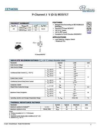
CET4435A www.VBsemi.tw P-Channel 35 V (D-S) MOSFET FEATURES PRODUCT SUMMARY Halogen-free According to IEC 61249-2-21 VDS (V) RDS(on) ( ) ID (A)d Qg (Typ.) Definition 0.050 at VGS = - 10 V - 6.2 TrenchFET Power MOSFET - 35 9.8 nC 0.060 at VGS = - 4.5 V - 5.1 100 % Rg Tested 100 % UIS Tested Compliant to RoHS Directive 2002/95/EC S APPLICATIONS
ap4435gm.pdf

AP4435GM www.VBsemi.tw P-Channel 30-V (D-S) MOSFET FEATURES PRODUCT SUMMARY Halogen-free According to IEC 61249-2-21 VDS (V) RDS(on) ( ) ID (A)d Qg (Typ.) Definition 0.018 at VGS = - 10 V - 9.0 TrenchFET Power MOSFET - 30 13 nC 100 % Rg Tested 0.024 at VGS = - 4.5 V - 7.8 APPLICATIONS Load Switch Battery Switch S SO-8 S 1 8 D G S D 2 7 S 3 6 D
cem4435a.pdf

CEM4435A www.VBsemi.tw P-Channel 30-V (D-S) MOSFET FEATURES PRODUCT SUMMARY Halogen-free According to IEC 61249-2-21 VDS (V) RDS(on) ( ) ID (A)d Qg (Typ.) Definition 0.018 at VGS = - 10 V - 9.0 TrenchFET Power MOSFET - 30 13 nC 100 % Rg Tested 0.024 at VGS = - 4.5 V - 7.8 APPLICATIONS Load Switch Battery Switch S SO-8 S 1 8 D G S D 2 7 S 3 6 D
irf4435tr.pdf
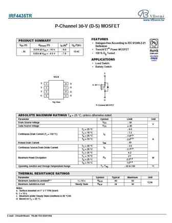
IRF4435TR www.VBsemi.tw P-Channel 30-V (D-S) MOSFET FEATURES PRODUCT SUMMARY Halogen-free According to IEC 61249-2-21 VDS (V) RDS(on) ( ) ID (A)d Qg (Typ.) Definition 0.018 at VGS = - 10 V - 9.0 TrenchFET Power MOSFET - 30 13 nC 100 % Rg Tested 0.024 at VGS = - 4.5 V - 7.8 APPLICATIONS Load Switch Battery Switch S SO-8 S 1 8 D G S D 2 7 S 3 6 D
fds4435bz.pdf
FDS4435BZ www.VBsemi.tw P-Channel 30-V (D-S) MOSFET FEATURES PRODUCT SUMMARY Halogen-free According to IEC 61249-2-21 VDS (V) RDS(on) ( ) ID (A)d Qg (Typ.) Definition 0.018 at VGS = - 10 V - 9.0 TrenchFET Power MOSFET - 30 13 nC 100 % Rg Tested 0.024 at VGS = - 4.5 V - 7.8 APPLICATIONS Load Switch Battery Switch S SO-8 S 1 8 D G S D 2 7 S 3 6 D
si4435dy-t1-e3.pdf
SI4435DY-T1-E3 www.VBsemi.tw P-Channel 30-V (D-S) MOSFET FEATURES PRODUCT SUMMARY Halogen-free According to IEC 61249-2-21 VDS (V) RDS(on) ( ) ID (A)d Qg (Typ.) Definition 0.018 at VGS = - 10 V - 9.0 TrenchFET Power MOSFET - 30 13 nC 100 % Rg Tested 0.024 at VGS = - 4.5 V - 7.8 APPLICATIONS Load Switch Battery Switch S SO-8 S 1 8 D G S D 2 7 S 3
si4435bdy.pdf

SI4435BDY www.VBsemi.tw P-Channel 30-V (D-S) MOSFET FEATURES PRODUCT SUMMARY Halogen-free According to IEC 61249-2-21 VDS (V) RDS(on) ( ) ID (A)d Qg (Typ.) Definition 0.018 at VGS = - 10 V - 9.0 TrenchFET Power MOSFET - 30 13 nC 100 % Rg Tested 0.024 at VGS = - 4.5 V - 7.8 APPLICATIONS Load Switch Battery Switch S SO-8 S 1 8 D G S D 2 7 S 3 6 D
hm4435b.pdf

HM4435B P-Channel Enhancement Mode Power MOSFET D DESCRIPTION The HM4435B uses advanced trench technology to provide G excellent RDS(ON), low gate charge and operation with gate voltages as low as 4.5V. S Schematic diagram GENERAL FEATURES VDS = -30V,ID = -9.1A RDS(ON)
hm4435.pdf
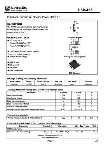
HM4435 P-Channel Enhancement Mode Power MOSFET D DESCRIPTION The HM4435 uses advanced trench technology to provide G excellent RDS(ON), low gate charge and operation with gate voltages as low as 4.5V. S Schematic diagram GENERAL FEATURES VDS = -30V,ID = -9.1A RDS(ON)
ap4435b.pdf
AP4435B -30V P-Channel Enhancement Mode MOSFET Description The AP4435B uses advanced trench technology to provide excellent R , low gate charge and DS(ON) operation with gate voltages as low as 4.5V. This device is suitable for use as a Battery protection or in other Switching application. General Features V = -30V I =-9.3A DS D R
ap4435a.pdf
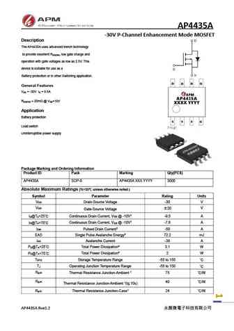
AP4435A -30V P-Channel Enhancement Mode MOSFET Description The AP4435A uses advanced trench technology to provide excellent RDS(ON), low gate charge and operation with gate voltages as low as 2.5V. This device is suitable for use as a Battery protection or in other Switching application. General Features VDS = -30V ID = 9.5A RDS(ON)
Otros transistores... 2021, 2026, 2341, 4401, 4402, 4407, 4409, 4410, AON7408, 4501, 4542, 4606, 4611, 4612, 4616, 4622, 4803
Parámetros del MOSFET. Cómo se afectan entre sí.
🌐 : EN ES РУ

Liste
Recientemente añadidas las descripciónes de los transistores:
MOSFET: BC2301 | BC1012W | BC1012T | BC1012 | 2SK3019WT | 2SK3019W | 2SK3018WT | CS95118 | CS85105A | CS75N45 | CS72N12 | CS55N50 | CS48N75A | CS40N27 | MSQ60P04D | MSQ40P07D
Popular searches
k b778 transistor | 2n5133 datasheet | 2sa726 transistor | 7506 mosfet | irlr8726 datasheet | ru7088r mosfet | mp40 transistor | fgpf4636 datasheet