4501 MOSFET Equivalente. Reemplazo. Hoja de especificaciones. Principales características
Número de Parte: 4501
Tipo de FET: MOSFET
Polaridad de transistor: NP
ESPECIFICACIONES MÁXIMAS
Pdⓘ - Máxima disipación de potencia: 2.5 W
|Vds|ⓘ - Voltaje máximo drenador-fuente: 30 V
|Vgs|ⓘ - Voltaje máximo fuente-puerta: 20 V
|Id|ⓘ - Corriente continua de drenaje: 7 A
Tjⓘ - Temperatura máxima de unión: 150 °C
CARACTERÍSTICAS ELÉCTRICAS
RDSonⓘ - Resistencia estado encendido drenaje a fuente: 0.018 Ohm
Encapsulados: SOP8
Búsqueda de reemplazo de 4501 MOSFET
- Selecciónⓘ de transistores por parámetros
4501 datasheet
4501.pdf
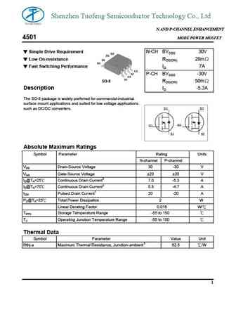
Shenzhen Tuofeng Semiconductor Technology Co., Ltd N AND P-CHANNEL ENHANCEMENT 4501 MODE POWER MOSFET Simple Drive Requirement N-CH BVDSS 30V D2 D2 Low On-resistance RDS(ON) 28m D1 D1 Fast Switching Performance ID 7A G2 S2 P-CH BVDSS -30V G1 S1 SO-8 RDS(ON) 50m Description ID -5.3A The SO-8 package is widely preferred for commercial-industrial surface mount app
pmp4501v g y.pdf
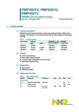
PMP4501V; PMP4501G; PMP4501Y NPN/NPN matched double transistors Rev. 04 28 August 2009 Product data sheet 1. Product profile 1.1 General description NPN/NPN matched double transistors in small Surface-Mounted Device (SMD) plastic packages. The transistors in the SOT666 and SOT363 (SC-88) packages are fully isolated internally. Table 1. Product overview Type number Package NPN/NPN
mp4501.pdf
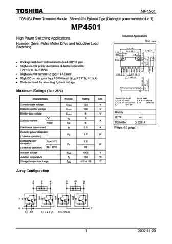
MP4501 TOSHIBA Power Transistor Module Silicon NPN Epitaxial Type (Darlington power transistor 4 in 1) MP4501 Industrial Applications High Power Switching Applications. Unit mm Hammer Drive, Pulse Motor Drive and Inductive Load Switching. Package with heat sink isolated to lead (SIP 12 pin) High collector power dissipation (4 devices operation) P = 5 W (Ta = 25 C
ki4501dy.pdf
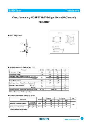
SMD Type IC SMD Type Transistors Complementary MOSFET Half-Bridge (N- and P-Channel) KI4501DY PIN Configuration Absolute Maximum Ratings TA =25 Parameter Symbol N-Channel P-Channel Unit Drain-Source Voltage VDS 30 -8 V Gate-Source Voltage VGS 20 8 V Continuous Drain Current (TJ = 150 )* TA =25 9 6.2 A ID TA =70 7.4 5.0 A Pulsed Drain Current IDM 30 20 A Continuous Source Current (D
ki4501ady.pdf
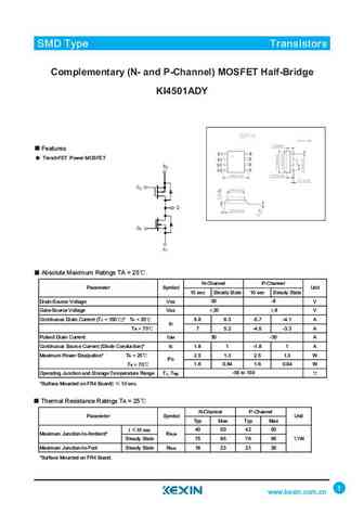
SMD Type IC SMD Type Transistors Complementary (N- and P-Channel) MOSFET Half-Bridge KI4501ADY Features TrenchFET Power MOSFET Absolute Maximum Ratings TA = 25 N-Channel P-Channel Parameter Symbol Unit 10 sec Steady State 10 sec Steady State Drain-Source Voltage VDS 30 -8 V Gate-Source Voltage VGS 20 8 V Continuous Drain Current (TJ = 150 )* TA =25 8.8 6.3 -5.7 -4.1 A ID TA =70 7
fds4501h.pdf
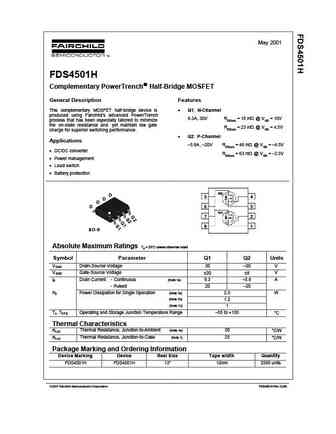
May 2001 FDS4501H Complementary PowerTrench Half-Bridge MOSFET General Description Features This complementary MOSFET half-bridge device is Q1 N-Channel produced using Fairchild s advanced PowerTrench 9.3A, 30V RDS(on) = 18 m @ VGS = 10V process that has been especially tailored to minimize the on-state resistance and yet maintain low gate RDS(on) = 23 m @ VGS =
ne450184c.pdf
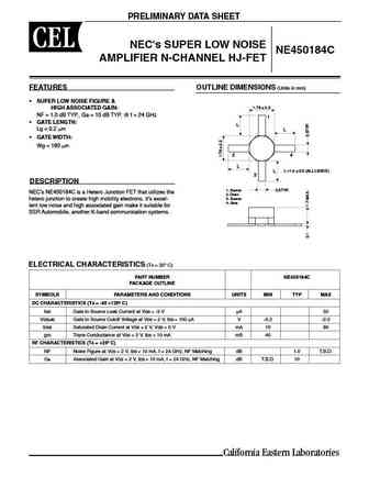
PRELIMINARY DATA SHEET NEC's SUPER LOW NOISE NE450184C AMPLIFIER N-CHANNEL HJ-FET FEATURES OUTLINE DIMENSIONS (Units in mm) SUPER LOW NOISE FIGURE & 1.78 0.2 HIGH ASSOCIATED GAIN NF = 1.0 dB TYP., Ga = 10 dB TYP. @ f = 24 GHz 1 GATE LENGTH L Lg
pmp4501v pmp4501g pmp4501y.pdf

Important notice Dear Customer, On 7 February 2017 the former NXP Standard Product business became a new company with the tradename Nexperia. Nexperia is an industry leading supplier of Discrete, Logic and PowerMOS semiconductors with its focus on the automotive, industrial, computing, consumer and wearable application markets In data sheets and application notes which still contain
pmp4501v.pdf

PMP4501V; PMP4501G; PMP4501Y NPN/NPN matched double transistors Rev. 04 28 August 2009 Product data sheet 1. Product profile 1.1 General description NPN/NPN matched double transistors in small Surface-Mounted Device (SMD) plastic packages. The transistors in the SOT666 and SOT363 (SC-88) packages are fully isolated internally. Table 1. Product overview Type number Package NPN/NPN
pmp4501g.pdf

PMP4501V; PMP4501G; PMP4501Y NPN/NPN matched double transistors Rev. 04 28 August 2009 Product data sheet 1. Product profile 1.1 General description NPN/NPN matched double transistors in small Surface-Mounted Device (SMD) plastic packages. The transistors in the SOT666 and SOT363 (SC-88) packages are fully isolated internally. Table 1. Product overview Type number Package NPN/NPN
pmp4501y.pdf

PMP4501V; PMP4501G; PMP4501Y NPN/NPN matched double transistors Rev. 04 28 August 2009 Product data sheet 1. Product profile 1.1 General description NPN/NPN matched double transistors in small Surface-Mounted Device (SMD) plastic packages. The transistors in the SOT666 and SOT363 (SC-88) packages are fully isolated internally. Table 1. Product overview Type number Package NPN/NPN
pmp4501qas.pdf
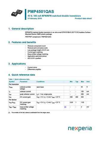
PMP4501QAS 45 V, 100 mA NPN/NPN matched double transistors 9 February 2018 Product data sheet 1. General description NPN/NPN matched double transistors in an ultra small DFN1010B-6 (SOT1216) leadless Surface- Mounted Device (SMD) plastic package. PNP/PNP complement PMP5501QAS 2. Features and benefits Reduces component count Reduces pick and place costs Low package height
si4501bdy.pdf
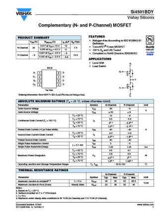
Si4501BDY Vishay Siliconix Complementary (N- and P-Channel) MOSFET FEATURES PRODUCT SUMMARY Halogen-free According to IEC 61249-2-21 VDS (V) RDS(on) ( ) ID (A)a Qg (Typ.) Definition 0.017 at VGS = 10 V 12 TrenchFET Power MOSFET N-Channel 30 7.9 0.020 at VGS = 4.5 V 11 100 % Rg and UIS Tested 0.027 at VGS = - 4.5 V - 8 Compliant to RoHS Directive 2002/95
si4501ad.pdf
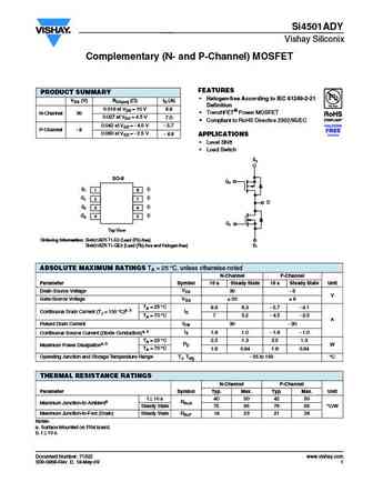
Si4501ADY Vishay Siliconix Complementary (N- and P-Channel) MOSFET FEATURES PRODUCT SUMMARY Halogen-free According to IEC 61249-2-21 VDS (V) RDS(on) ( )ID (A) Definition 0.018 at VGS = 10 V 8.8 TrenchFET Power MOSFET N-Channel 30 0.027 at VGS = 4.5 V 7.0 Compliant to RoHS Directive 2002/95/EC 0.042 at VGS = - 4.5 V - 5.7 P-Channel - 8 0.060 at VGS = - 2.5
si4501dy.pdf
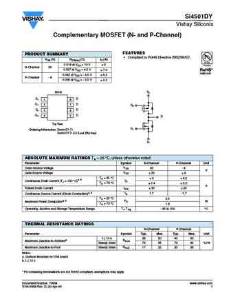
Si4501DY Vishay Siliconix Complementary MOSFET (N- and P-Channel) FEATURES PRODUCT SUMMARY Compliant to RoHS Directive 2002/95/EC VDS (V) RDS(on) ( )ID (A) 0.018 at VGS = 10 V 9 N-Channel 30 0.027 at VGS = 4.5 V 7.4 0.042 at VGS = - 4.5 V 6.2 P-Channel - 8 0.060 at VGS = - 2.5 V 5.2 S2 SO-8 S D 1 1 8 G 1 2 D 7 G2 S D 2 3 6 G 2 4 D 5 D
nsvt45010mw6t3g.pdf
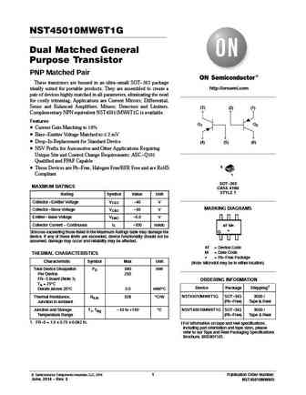
NST45010MW6T1G Dual Matched General Purpose Transistor PNP Matched Pair These transistors are housed in an ultra-small SOT-363 package http //onsemi.com ideally suited for portable products. They are assembled to create a pair of devices highly matched in all parameters, eliminating the need for costly trimming. Applications are Current Mirrors; Differential, Sense and Balanced Amplifi
ntr4501nt1.pdf

NTR4501N, NSTR4501N Power MOSFET 20 V, 3.2 A, Single N-Channel, SOT-23 Features Leading Planar Technology for Low Gate Charge / Fast Switching http //onsemi.com 2.5 V Rated for Low Voltage Gate Drive SOT-23 Surface Mount for Small Footprint V(BR)DSS RDS(on) Typ ID Max (Note 1) NSTR Prefix for Automotive and Other Applications Requiring 70 mW @ 4.5 V 3.6 A Unique Site
nst45011mw6t1g nsvt45011mw6t3g.pdf

NST45011MW6T1G, NSVT45011MW6T3G Dual Matched General Purpose Transistor NPN Matched Pair http //onsemi.com These transistors are housed in an ultra-small SOT-363 package ideally suited for portable products. They are assembled to create a pair of devices highly matched in all parameters, eliminating the need for costly trimming. Applications are Current Mirrors; Differential, Sense an
ntr4501n nvr4501n.pdf
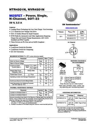
NTR4501N, NVR4501N MOSFET Power, Single, N-Channel, SOT-23 20 V, 3.2 A Features www.onsemi.com Leading Planar Technology for Low Gate Charge / Fast Switching 2.5 V Rated for Low Voltage Gate Drive V(BR)DSS RDS(on) Typ ID Max (Note 1) SOT-23 Surface Mount for Small Footprint 70 mW @ 4.5 V 3.6 A NVR Prefix for Automotive and Other Applications Requiring 20 V Uniqu
ntr4501n.pdf
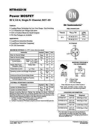
NTR4501N Power MOSFET 20 V, 3.2 A, Single N-Channel, SOT-23 Features Leading Planar Technology for Low Gate Charge / Fast Switching http //onsemi.com 2.5 V Rated for Low Voltage Gate Drive V(BR)DSS RDS(on) Typ ID Max SOT-23 Surface Mount for Small Footprint (Note 1) Pb-Free Packages are Available 70 mW @ 4.5 V 3.6 A 20 V Applications 88 mW @ 2.5 V 3.1 A Load/P
nsvt45010mw6t1g.pdf

NST45010MW6T1G Dual Matched General Purpose Transistor PNP Matched Pair These transistors are housed in an ultra-small SOT-363 package http //onsemi.com ideally suited for portable products. They are assembled to create a pair of devices highly matched in all parameters, eliminating the need for costly trimming. Applications are Current Mirrors; Differential, Sense and Balanced Amplifi
nst45010mw6t1g.pdf

NST45010MW6T1G Dual Matched General Purpose Transistor PNP Matched Pair These transistors are housed in an ultra-small SOT-363 package http //onsemi.com ideally suited for portable products. They are assembled to create a pair of devices highly matched in all parameters, eliminating the need for costly trimming. Applications are Current Mirrors; Differential, Sense and Balanced Amplifi
nsvt45011mw6t3g.pdf
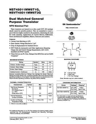
NST45011MW6T1G, NSVT45011MW6T3G Dual Matched General Purpose Transistor NPN Matched Pair http //onsemi.com These transistors are housed in an ultra-small SOT-363 package ideally suited for portable products. They are assembled to create a pair of devices highly matched in all parameters, eliminating the need for costly trimming. Applications are Current Mirrors; Differential, Sense an
nst45010mw6-d.pdf
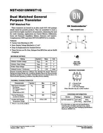
NST45010MW6T1G Dual Matched General Purpose Transistor PNP Matched Pair These transistors are housed in an ultra-small SOT-363 package http //onsemi.com ideally suited for portable products. They are assembled to create a pair of devices highly matched in all parameters, eliminating the need for costly trimming. Applications are Current Mirrors; Differential, Sense and Balanced Amplifi
fds4501h.pdf

Is Now Part of To learn more about ON Semiconductor, please visit our website at www.onsemi.com Please note As part of the Fairchild Semiconductor integration, some of the Fairchild orderable part numbers will need to change in order to meet ON Semiconductor s system requirements. Since the ON Semiconductor product management systems do not have the ability to manage part nomenclatur
nilms4501n nilms4501nr2 nilms4501nr2g.pdf
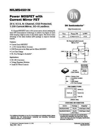
NILMS4501N Power MOSFET with Current Mirror FET 24 V, 9.5 A, N-Channel, ESD Protected, 1 250 Current Mirror, SO-8 Leadless http //onsemi.com N-Channel MOSFET with 1 250 current mirror device utilizing the latest ON Semiconductor technology to achieve low figure of merit VDSS RDS(on) Typ ID MAX while keeping a high accuracy in the linear region. This device takes 24 V 12 mW @ 4.5 V 9.5
nvr4501n.pdf
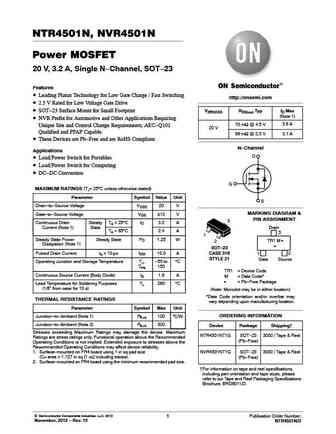
NTR4501N, NVR4501N Power MOSFET 20 V, 3.2 A, Single N-Channel, SOT-23 Features Leading Planar Technology for Low Gate Charge / Fast Switching http //onsemi.com 2.5 V Rated for Low Voltage Gate Drive SOT-23 Surface Mount for Small Footprint V(BR)DSS RDS(on) Typ ID Max (Note 1) NVR Prefix for Automotive and Other Applications Requiring 70 mW @ 4.5 V 3.6 A Unique Site an
nths4501n-d nths4501nt1 nths4501nt1g.pdf
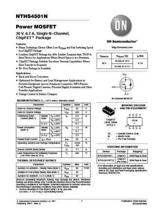
NTHS4501N Power MOSFET 30 V, 6.7 A, Single N-Channel, ChipFETt Package Features http //onsemi.com Planar Technology Device Offers Low RDS(on) and Fast Switching Speed in a ChipFET Package Leadless ChipFET Package has 40% Smaller Footprint than TSOP-6. V(BR)DSS RDS(on) Typ ID Max Ideal Device for Applications Where Board Space is at a Premium. 30 mW @ 10 V ChipFET Packag
nst45011mw6-d.pdf
NST45011MW6T1G Dual Matched General Purpose Transistor NPN Matched Pair These transistors are housed in an ultra-small SOT-363 package http //onsemi.com ideally suited for portable products. They are assembled to create a pair of devices highly matched in all parameters, eliminating the need for costly trimming. Applications are Current Mirrors; Differential, Sense and Balanced Amplifi
dsc4501.pdf
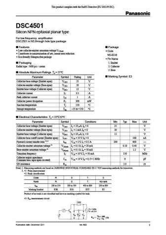
This product complies with the RoHS Directive (EU 2002/95/EC). DSC4501 Silicon NPN epitaxial planar type For low frequency amplification DSC2501 in NS through hole type package Features Package Low collector-emitter saturation voltage VCE(sat) Code Contributes to miniaturization of sets, mount area reduction NS-B2-B Eco-friendly Halogen-free package Pin N
2sc4501.pdf
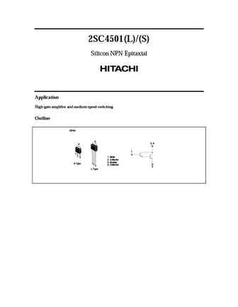
2SC4501(L)/(S) Silicon NPN Epitaxial Application High gain amplifier and medium speed switching Outline DPAK 4 2, 4 4 1 1 2 1. Base 3 2. Collector 3. Emitter S Type 12 4. Collector 3 3 L Type 2SC4501(L)/(S) Absolute Maximum Ratings (Ta = 25 C) Item Symbol Ratings Unit Collector to base voltage VCBO 30 V Collector to emitter voltage VCEO 30 V Emitter to base volta
ssg4501.pdf
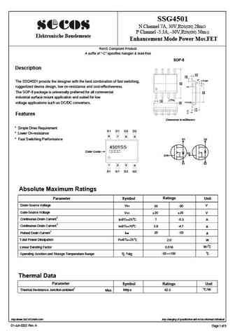
SSG4501 N Channel 7A, 30V,RDS(ON) 28m P Channel -5.3A, -30V,RDS(ON) 50m Elektronische Bauelemente Enhancement Mode Power Mos.FET RoHS Compliant Product SOP-8 Description 0.19 0.25 0.40 0.90 o 0.375 REF The SSG4501 provide the designer with the best combination of fast switching, 6.20 5.80 0.25 rugged
wtc4501.pdf
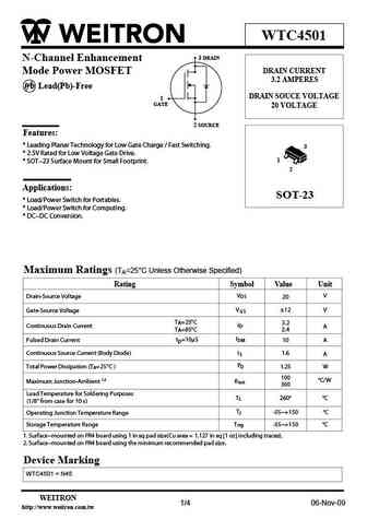
WTC4501 3 DRAIN N-Channel Enhancement DRAIN CURRENT Mode Power MOSFET 3.2 AMPERES P b Lead(Pb)-Free DRAIN SOUCE VOLTAGE 1 GATE 20 VOLTAGE 2 SOURCE Features * Leading Planar Technology for Low Gate Charge / Fast Switching. 3 * 2.5V Rated for Low Voltage Gate Drive. 1 * SOT-23 Surface Mount for Small Footprint. 2 Applications SOT-23 * Load/Power Switch for Portables. * Lo
wtk4501.pdf
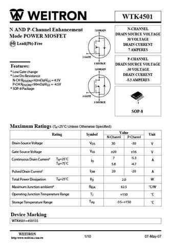
WTK4501 N-CHANNEL N AND P-Channel Enhancement 7,8 DRAIN DRAIN SOURCE VOLTAGE Mode POWER MOSFET 30 VOLTAGE P b Lead(Pb)-Free DRAIN CURRENT 7 AMPERES 2 GATE P-CHANNEL 1 SOURCE DRAIN SOURCE VOLTAGE Features 5,6 DRAIN -30 VOLTAGE * Low Gate change DRAIN CURRENT * Low On-Resistance N-CH RDS(ON)
w4501dw.pdf
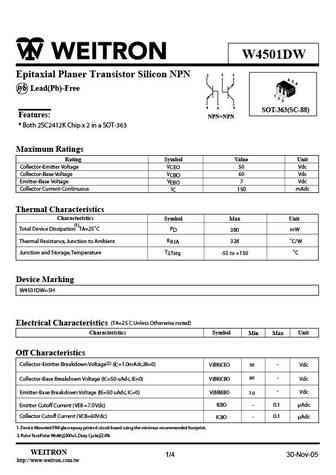
W4501DW 2 1 3 Epitaxial Planer Transistor Silicon NPN 6 5 4 P b Lead(Pb)-Free 1 2 3 4 5 6 SOT-363(SC-88) Features NPN+NPN * Both 2SC2412K Chip x 2 in a SOT-363 Maximum Ratings Rating Symbol Value Unit Collector-Emitter Voltage V 50 Vdc CEO Collector-Base Voltage VCBO 60 Vdc Emitter-Base Voltage VEBO 7 Vdc Collector Current-Continuous IC 150 mAdc Thermal Characteristics
ap4501gd.pdf
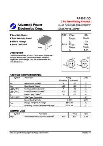
AP4501GD Pb Free Plating Product Advanced Power N AND P-CHANNEL ENHANCEMENT Electronics Corp. MODE POWER MOSFET Low Gate Charge N-CH BVDSS 30V D2 D2 D1 Fast Switching Speed RDS(ON) 28m D1 PDIP-8 Package ID 7A RoHS Compliant P-CH BVDSS -30V G2 S2 RDS(ON) 50m PDIP-8 G1 S1 ID -5.3A Description The Advanced Power MOSFETs from APEC provide the designer with t
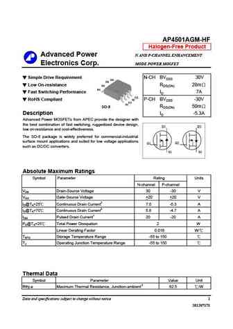
ap4501agem-hf.pdf
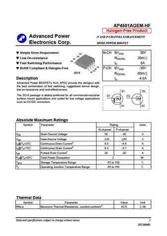
AP4501AGEM-HF Halogen-Free Product Advanced Power N AND P-CHANNEL ENHANCEMENT Electronics Corp. MODE POWER MOSFET Simple Drive Requirement N-CH BVDSS 30V D2 D2 Low On-resistance RDS(ON) 20m D1 D1 Fast Switching Performance ID 8A G2 RoHS Compliant & Halogen-Free P-CH BVDSS -30V S2 G1 S1 SO-8 RDS(ON) 60m Description ID -4.6A Advanced Power MOSFETs from APEC
ap4501agm.pdf
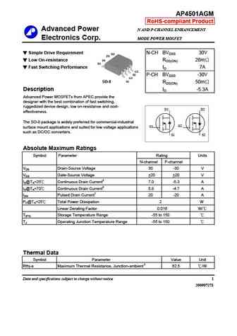
AP4501AGM RoHS-compliant Product Advanced Power N AND P-CHANNEL ENHANCEMENT Electronics Corp. MODE POWER MOSFET Simple Drive Requirement N-CH BVDSS 30V D2 D2 Low On-resistance D1 RDS(ON) 28m D1 Fast Switching Performance ID 7A G2 S2 P-CH BVDSS -30V G1 S1 SO-8 RDS(ON) 50m Description ID -5.3A Advanced Power MOSFETs from APEC provide the designer with the best co
ap4501gh-hf.pdf
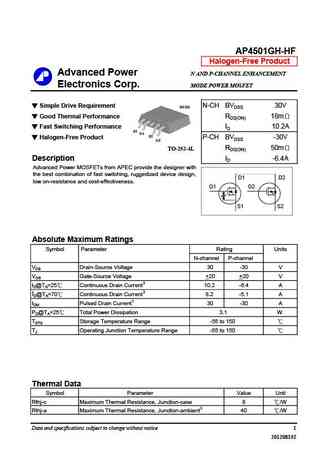
AP4501GH-HF Halogen-Free Product Advanced Power N AND P-CHANNEL ENHANCEMENT Electronics Corp. MODE POWER MOSFET Simple Drive Requirement N-CH BVDSS 30V D1/D2 Good Thermal Performance RDS(ON) 18m Fast Switching Performance ID 10.2A S1 G1 S2 Halogen-Free Product P-CH BVDSS -30V G2 RDS(ON) 50m TO-252-4L Description ID -6.4A Advanced Power MOSFETs from APEC provi
ap4501cgm-hf.pdf
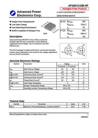
AP4501CGM-HF Halogen-Free Product Advanced Power N AND P-CHANNEL ENHANCEMENT Electronics Corp. MODE POWER MOSFET Simple Drive Requirement N-CH BVDSS 30V D2 D2 Low Gate Charge D1 RDS(ON) 25m D1 Fast Switching Performance ID 7A G2 S2 RoHS Compliant & Halogen-Free P-CH BVDSS -30V G1 S1 SO-8 RDS(ON) 80m Description ID -4A Advanced Power MOSFETs from APEC provid
ap4501agey-hf.pdf
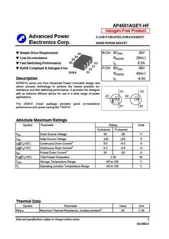
AP4501AGEY-HF Halogen-Free Product Advanced Power N AND P-CHANNEL ENHANCEMENT Electronics Corp. MODE POWER MOSFET Simple Drive Requirement N-CH BVDSS 30V D2 D2 Low On-resistance RDS(ON) 20m D1 D1 G2 Fast Switching Performance ID 6.5A S2 RoHS Compliant & Halogen-Free P-CH BVDSS -30V G1 S1 2928-8 RDS(ON) 45m Description ID -4.5A AP4501A series are from Advan
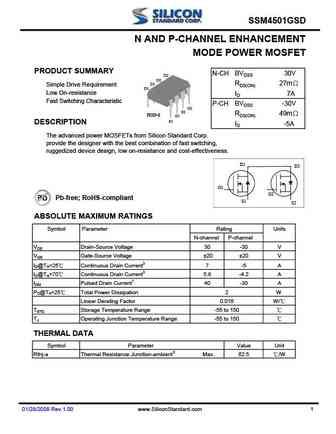
ap4501gsd.pdf
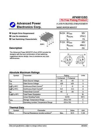
AP4501GSD Pb Free Plating Product Advanced Power N AND P-CHANNEL ENHANCEMENT Electronics Corp. MODE POWER MOSFET D2 Simple Drive Requirement N-CH BVDSS 30V D2 D1 Low On-resistance D1 RDS(ON) 27m Fast Switching Characteristic ID 7A G2 P-CH BVDSS -30V S2 PDIP-8 G1 RDS(ON) 49m S1 Description ID -5A The Advanced Power
ap4501agm-hf.pdf
AP4501AGM-HF Halogen-Free Product Advanced Power N AND P-CHANNEL ENHANCEMENT Electronics Corp. MODE POWER MOSFET Simple Drive Requirement N-CH BVDSS 30V D2 D2 Low On-resistance RDS(ON) 28m D1 D1 Fast Switching Performance ID 7A G2 RoHS Compliant P-CH BVDSS -30V S2 G1 S1 RDS(ON) 50m SO-8 Description ID -5.3A Advanced Power MOSFETs from APEC provide the desi
ap4501gm-hf.pdf
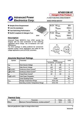
AP4501GM-HF Halogen-Free Product Advanced Power N AND P-CHANNEL ENHANCEMENT Electronics Corp. MODE POWER MOSFET Simple Drive Requirement N-CH BVDSS 30V D2 D2 Low On-resistance RDS(ON) 28m D1 D1 Fast Switching Performance ID 7A G2 RoHS Compliant & Halogen-Free P-CH BVDSS -30V S2 G1 S1 SO-8 RDS(ON) 50m Description ID -5.3A Advanced Power MOSFETs from APEC pro
ap4501gm.pdf
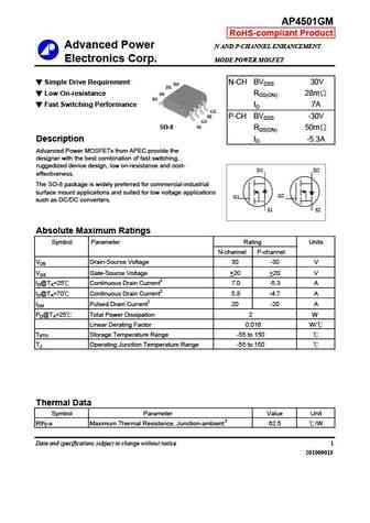
AP4501GM RoHS-compliant Product Advanced Power N AND P-CHANNEL ENHANCEMENT Electronics Corp. MODE POWER MOSFET Simple Drive Requirement N-CH BVDSS 30V D2 D2 Low On-resistance D1 RDS(ON) 28m D1 Fast Switching Performance ID 7A G2 S2 P-CH BVDSS -30V G1 S1 SO-8 RDS(ON) 50m Description ID -5.3A Advanced Power MOSFETs from APEC provide the designer with the best com
mtc4501q8.pdf
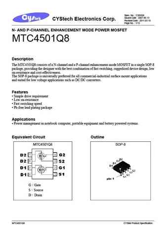
Spec. No. C385Q8 Issued Date 2007.06.13 CYStech Electronics Corp. Revised Date 2011.03.18 Page No. 1/12 N- AND P-CHANNEL ENHANCEMENT MODE POWER MOSFET MTC4501Q8 Description The MTC4501Q8 consists of a N-channel and a P-channel enhancement-mode MOSFET in a single SOP-8 package, providing the designer with the best combination of fast switching, ruggedized device design,
sts4501.pdf
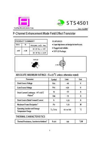
Green Product S TS 4501 S amHop Microelectronics C orp. t. 12,2007 c O P-Channel E nhancement Mode Field E ffect Transistor PR ODUC T S UMMAR Y F E ATUR E S VDS S ID S uper high dense cell design for low R DS (ON). R DS (ON) ( m ) Max R ugged and reliable. 65 @ VG S = -10V -40V -3.5A S OT-23 Package. 85 @ VG S = -4.5V D S OT-23 G S ABS OLUTE MAXIMUM R ATINGS (TA=25 C un
ln4501lt1g.pdf
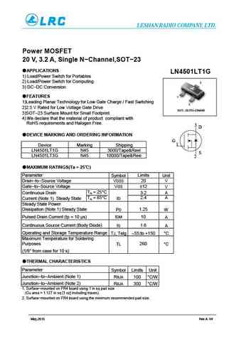
LESHAN RADIO COMPANY, LTD. Power MOSFET 20 V, 3.2 A, Single N-Channel,SOT-23 APPLICATIONS LN4501LT1G 1) Load/Power Switch for Portables 2) Load/Power Switch for Computing 3 3) DC-DC Conversion FEATURES 1 1)Leading Planar Technology for Low Gate Charge / Fast Switching 2 2)2.5 V Rated for Low Voltage Gate Drive SOT 23 (TO 236AB) 3)SOT-23 Surface Mount for Small Footprin
sm4501psk.pdf
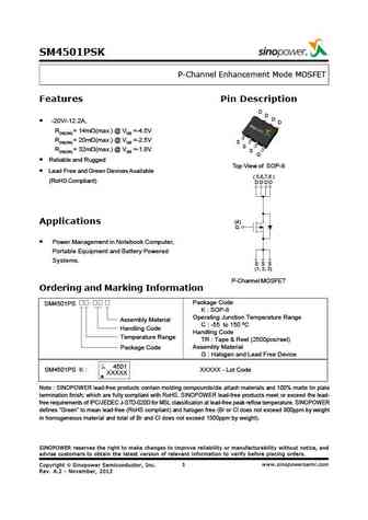
SM4501PSK P-Channel Enhancement Mode MOSFET Features Pin Description D D D -20V/-12.2A, D RDS(ON) = 14m (max.) @ VGS =-4.5V RDS(ON) = 20m (max.) @ VGS =-2.5V S S RDS(ON) = 32m (max.) @ VGS =-1.8V S G Reliable and Rugged Top View of SOP-8 Lead Free and Green Devices Available ( 5,6,7,8 ) (RoHS Compliant) D D D D (4) Applications G Power Management in Notebook Compu
ntr4501n.pdf
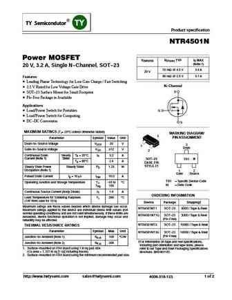
Product specification NTR4501N Power MOSFET V(BR)DSS RDS(on) TYP ID MAX (Note 1) 20 V, 3.2 A, Single N-Channel, SOT-23 70 mW @ 4.5 V 3.6 A 20 V 85 mW @ 2.5 V 3.1 A Features Leading Planar Technology for Low Gate Charge / Fast Switching N-Channel 2.5 V Rated for Low Voltage Gate Drive D SOT-23 Surface Mount for Small Footprint Pb-Free Package is Available Applicat
kds4501h.pdf
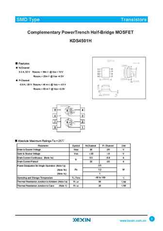
SMD Type IC SMD Type Transistors Complementary PowerTrench Half-Bridge MOSFET KDS4501H Features N-Channel 9.3A, 30V RDS(ON) = 18m @VGS =10 V RDS(ON) = 23m @VGS =4.5V P-Channel -5.6 A, -20 V RDS(ON) =46 m @VGS =- 4.5 V RDS(ON) =63m @VGS =-2.5V Absolute Maximum Ratings Ta = 25 Parameter Symbol N-Channel P- Channel Unit Drain to Source Voltage VDSS 30 -20 V Gate to Source Voltage VGS
chm4501jgp.pdf
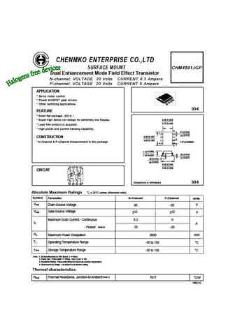
CHENMKO ENTERPRISE CO.,LTD SURFACE MOUNT CHM4501JGP Dual Enhancement Mode Field Effect Transistor N-channel VOLTAGE 20 Volts CURRENT 8.3 Ampere P-channel VOLTAGE 20 Volts CURRENT 5 Ampere APPLICATION * Servo motor control. * Power MOSFET gate drivers. * Other switching applications. SO-8 FEATURE * Small flat package. (SO-8 ) ( ) * Super high dense cell design for extremely low R
ssm4501gm.pdf
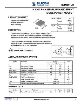
SSM4501GM N AND P-CHANNEL ENHANCEMENT MODE POWER MOSFET PRODUCT SUMMARY N-CH BVDSS 30V D2 Simple Drive Requirement D2 RDS(ON) 28m D1 Low On-resistance D1 ID 7A Fast Switching G2 P-CH BVDSS -30V S2 G1 SO-8 RDS(ON) 50m S1 DESCRIPTION ID -5.3A The advanced power MOSFETs from Silicon Standard Corp. provide the designer with the best combination of fast switching,
ssm4501gsd.pdf
SSM4501GSD N AND P-CHANNEL ENHANCEMENT MODE POWER MOSFET PRODUCT SUMMARY N-CH BVDSS 30V D2 D2 D1 RDS(ON) 27m Simple Drive Requirement D1 Low On-resistance ID 7A Fast Switching Characteristic P-CH BVDSS -30V G2 S2 RDS(ON) 49m PDIP-8 G1 S1 DESCRIPTION ID -5A The advanced power MOSFETs from Silicon Standard Corp. provide the designer with the best combination of
ap4501agm.pdf
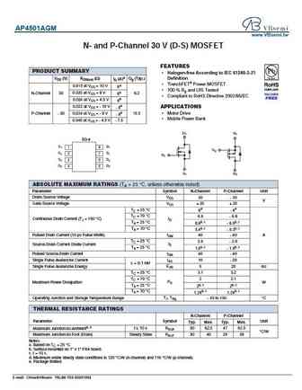
AP4501AGM www.VBsemi.tw N- and P-Channel 30 V (D-S) MOSFET FEATURES PRODUCT SUMMARY Halogen-free According to IEC 61249-2-21 VDS (V) RDS(on) ( ) Definition ID (A)a Qg (Typ.) TrenchFET Power MOSFET 0.018 at VGS = 10 V 8e 100 % Rg and UIS Tested N-Channel 30 0.020 at VGS = 8 V 8e 6.2 Compliant to RoHS Directive 2002/95/EC 0.024 at VGS = 4.5 V 8e 0.032 at VG
Otros transistores... 2026 , 2341 , 4401 , 4402 , 4407 , 4409 , 4410 , 4435 , 2N7002 , 4542 , 4606 , 4611 , 4612 , 4616 , 4622 , 4803 , 4812 .
🌐 : EN ES РУ

Liste
Recientemente añadidas las descripciónes de los transistores:
MOSFET: ASD80R750E | ASD70R950E | ASD70R600E | ASD70R380E | ASD65R850E | ASD65R550E | ASD65R350E | ASD65R300E | ASD65R280E | ASD65R270E | ASD60R330E | ASD60R280E | ASB80R750E | ASB70R380E | ASB65R300E | ASB65R220E
Popular searches
2n5133 datasheet | 2sa726 transistor | 7506 mosfet | irlr8726 datasheet | ru7088r mosfet | mp40 transistor | fgpf4636 datasheet | 2sc1945