4606 MOSFET Equivalente. Reemplazo. Hoja de especificaciones. Principales características
Número de Parte: 4606
Tipo de FET: MOSFET
Polaridad de transistor: NP
ESPECIFICACIONES MÁXIMAS
Pdⓘ - Máxima
disipación de potencia: 2 W
|Vds|ⓘ - Voltaje máximo drenador-fuente: 30 V
|Vgs|ⓘ - Voltaje máximo fuente-puerta: 20 V
|Id|ⓘ - Corriente continua
de drenaje: 6.9 A
Tjⓘ - Temperatura máxima de unión: 150 °C
CARACTERÍSTICAS ELÉCTRICAS
RDSonⓘ - Resistencia estado encendido drenaje a fuente: 0.028 Ohm
Encapsulados: SOP8
Búsqueda de reemplazo de 4606 MOSFET
- Selecciónⓘ de transistores por parámetros
4606 datasheet
..1. Size:1380K shenzhen
4606.pdf 
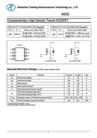
Shenzhen Tuofeng Semiconductor Technology co., LTD 4606 Complementary High Density Trench MOSFET PRODUCT SUMMARY (N-Channel) PRODUCT SUMMARY (P-Channel) VDSS ID RDS(on) (m-ohm) Max VDSS ID RDS(on) (m-ohm) Max 28 @ VGS = 10 V,ID=6.9A 50 @ VGS = -10V,ID=- 6.0 A 6.9A -6.0 A 30V -30V 42 @ VGS = 4.5V,ID=5.0A 80@VGS = -4.5V, ID=- 5.0A Absolute Maximum Ratings (TA=25oC, unless otherwise
..2. Size:3723K cn tuofeng
4606.pdf
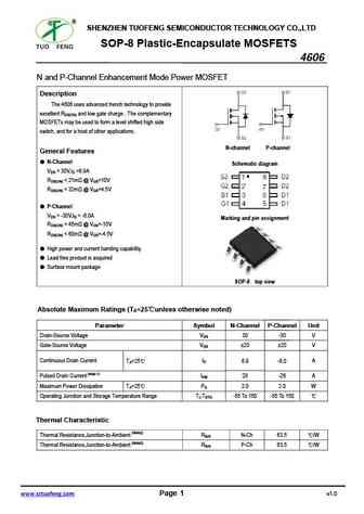
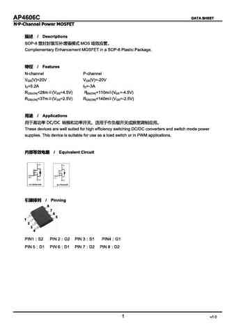
SHENZHEN TUOFENG SEMICONDUCTOR TECHNOLOGY CO.,LTD SOP-8 Plastic-Encapsulate MOSFETS 4606 N and P-Channel Enhancement Mode Power MOSFET Description The 4606 uses advanced trench technology to provide excellent RDS(ON) and low gate charge . The complementary MOSFETs may be used to form a level shifted high side switch, and for a host of other applications. N-channel P-channel Gen
0.1. Size:149K toshiba
rn4606.pdf
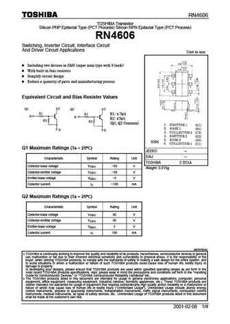
RN4606 TOSHIBA Transistor Silicon PNP Epitaxial Type (PCT Process) Silicon NPN Epitaxial Type (PCT Process) RN4606 Switching, Inverter Circuit, Interface Circuit And Driver Circuit Applications Unit in mm Including two devices in SM6 (super mini type with 6 leads) With built-in bias resistors Simplify circuit design Reduce a quantity of parts and manufacturing process
0.2. Size:48K panasonic
2sc4606.pdf
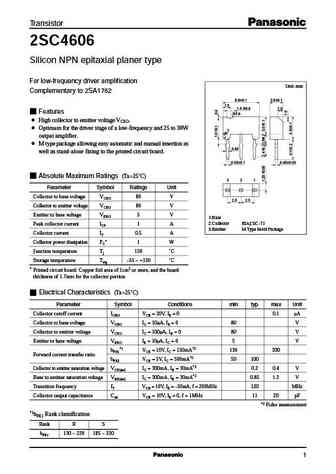
Transistor 2SC4606 Silicon NPN epitaxial planer type For low-frequency driver amplification Unit mm Complementary to 2SA1762 6.9 0.1 2.5 0.1 1.5 1.5 R0.9 1.0 Features R0.9 High collector to emitter voltage VCEO. Optimum for the driver stage of a low-frequency and 25 to 30W output amplifier. M type package allowing easy automatic and manual insertion as 0.85 well as stand-al
0.3. Size:52K panasonic
2sc4606 e.pdf

Transistor 2SC4606 Silicon NPN epitaxial planer type For low-frequency driver amplification Unit mm Complementary to 2SA1762 6.9 0.1 2.5 0.1 1.5 1.5 R0.9 1.0 Features R0.9 High collector to emitter voltage VCEO. Optimum for the driver stage of a low-frequency and 25 to 30W output amplifier. M type package allowing easy automatic and manual insertion as 0.85 well as stand-al
0.4. Size:7744K jiangsu
cjq4606.pdf
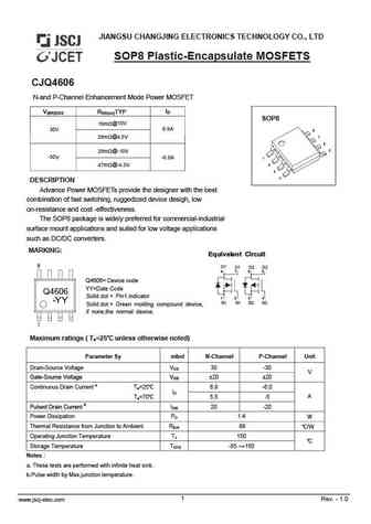
JIANGSU CHANGJING ELECTRONICS TECHNOLOGY CO., LTD SOP8 Plastic-Encapsulate MOSFETS CJQ4606 N-and P-Channel Enhancement Mode Power MOSFET ID V(BR)DSS RDS(on)TYP SOP8 19m @10V 6.9A 30V 28m @4.5V 29m @-10V -30 V -6.0A 47m @-4.5V DESCRIPTION Advance Power MOSFETs provide the designer with the best combination of fast switching, ruggedized device desigh, low on-r
0.5. Size:545K aosemi
ao4606.pdf
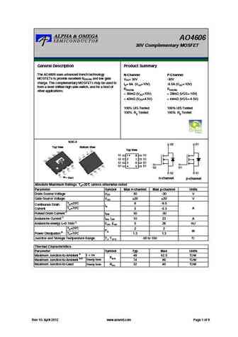
AO4606 30V Complementary MOSFET General Description Product Summary The AO4606 uses advanced trench technology N-Channel P-Channel MOSFETs to provide excellent RDS(ON) and low gate VDS= 30V -30V charge. The complementary MOSFETs may be used to ID= 6A (VGS=10V) -6.5A (VGS=-10V) form a level shifted high side switch, and for a host of RDS(ON) RDS(ON) other applications.
0.6. Size:200K ape
ap4606p.pdf
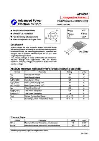
AP4606P Halogen-Free Product Advanced Power N-CHANNEL ENHANCEMENT MODE Electronics Corp. POWER MOSFET Simple Drive Requirement D BVDSS 40V Ultra-low On-resistance RDS(ON) 3.7m Fast Switching Characteristic ID3 125A G RoHS Compliant & Halogen-Free S Description AP4606 series are from Advanced Power innovated design and silicon process technology to achieve the lowes
0.7. Size:496K silikron
ssf4606.pdf
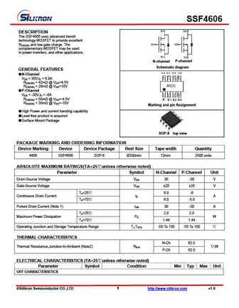
SSF4606 DESCRIPTION The SSF4606 uses advanced trench technology MOSFET to provide excellent RDS(ON) and low gate charge. The complementary MOSFET may be used in power inverters, and other applications. P-channel N-channel Schematic diagram GENERAL FEATURES N-Channel VDS = 30V,ID = 6.9A RDS(ON)
0.8. Size:1412K blue-rocket-elect
brcs4606hsc.pdf
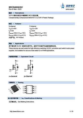
BRCS4606HSC Rev.B Mar.-2022 DATA SHEET / Descriptions SOP-8 MOS Complementary Enhancement MOSFET in a SOP-8 Plastic Package. / Features N-channel P-channel VDS(V)=30V VDS(V)=-30V ID=6.9A ID=-6.0A RDS(ON)
0.9. Size:2249K blue-rocket-elect
brcs4606sc.pdf
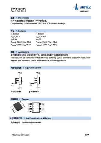
BRCS4606SC Rev.E Oct.-2018 DATA SHEET / Descriptions SOP-8 MOS Complementary Enhancement MOSFET in a SOP-8 Plastic Package. / Features N-channel P-channel VDS(V)=30V VDS(V)=-30V ID=6.9A ID=-6A RDS(ON)
0.10. Size:2601K kexin
ao4606.pdf
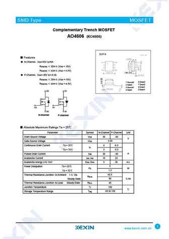
SMD Type MOSFET Complementary Trench MOSFET AO4606 (KO4606) SOP-8 Features N-Channel VDS=30V ID=6A RDS(ON) 30m (VGS = 10V) RDS(ON) 42m (VGS = 4.5V) 1.50 0.15 P-Channel VDS=-30V ID=-6.5A RDS(ON) 28m (VGS =-10V) 1 Source2 8 Drain2 RDS(ON) 44m (VGS =-4.5V) 7 Drain2 2 Gate2 6 Drain1 3 Source1 5 Drain1 4 Gate1 D2 D1 G2 G1 S2 S1 N-chann
0.11. Size:670K elm
elm14606aa.pdf
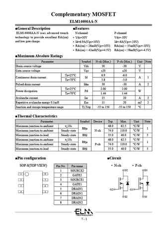
Complementary MOSFET ELM14606AA-N General Description Features ELM14606AA-N uses advanced trench N-channel P-channel technology to provide excellent Rds(on) Vds=30V Vds=-30V and low gate charge. Id=6.9A(Vgs=10V) Id=-6A(Vgs=-10V) Rds(on)
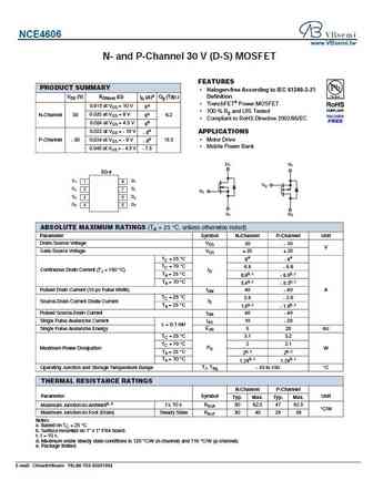
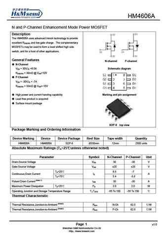
0.12. Size:397K ncepower
nce4606b.pdf
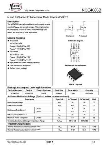
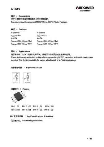
http //www.ncepower.com NCE4606B N and P-Channel Enhancement Mode Power MOSFET Description The NCE4606B uses advanced trench technology to provide excellent RDS(ON) and low gate charge . The complementary MOSFETs may be used to form a level shifted high side switch, and for a host of other applications. N-channel P-channel General Features N-Channel Schematic diagram VDS
0.13. Size:423K ncepower
nce4606a.pdf
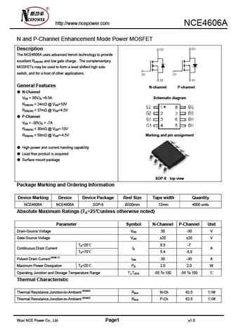
http //www.ncepower.com NCE4606A N and P-Channel Enhancement Mode Power MOSFET Description The NCE4606A uses advanced trench technology to provide excellent RDS(ON) and low gate charge . The complementary MOSFETs may be used to form a level shifted high side switch, and for a host of other applications. General Features N-channel P-channel N-Channel VDS = 30V,ID =6.5A Sc
0.14. Size:1122K ncepower
nce4606c.pdf
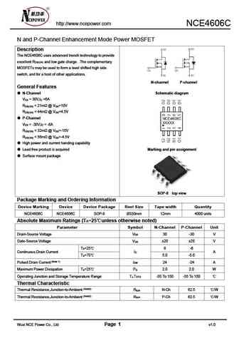
http //www.ncepower.com NCE4606C N and P-Channel Enhancement Mode Power MOSFET Description The NCE4606C uses advanced trench technology to provide excellent R and low gate charge . The complementary DS(ON) MOSFETs may be used to form a level shifted high side switch, and for a host of other applications. N-channel P-channel General Features N-Channel Schematic diagram V = 30V,I
0.15. Size:434K ncepower
nce4606.pdf
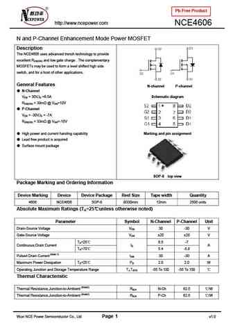
Pb Free Product http //www.ncepower.com NCE4606 N and P-Channel Enhancement Mode Power MOSFET Description The NCE4606 uses advanced trench technology to provide excellent RDS(ON) and low gate charge . The complementary MOSFETs may be used to form a level shifted high side switch, and for a host of other applications. General Features N-channel P-channel N-Channel VDS =
0.16. Size:60K sensitron
shd224605 shd224606.pdf
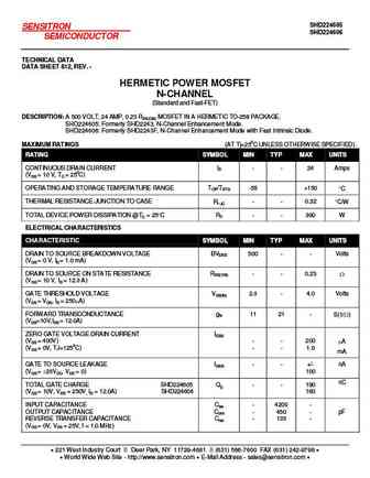
SHD224605 SENSITRON SHD224606 SEMICONDUCTOR TECHNICAL DATA DATA SHEET 812, REV. - HERMETIC POWER MOSFET N-CHANNEL (Standard and Fast-FET) DESCRIPTION A 500 VOLT, 24 AMP, 0.23 RDS(ON) MOSFET IN A HERMETIC TO-258 PACKAGE. SHD224605 Formerly SHD2243, N-Channel Enhancement Mode. SHD224606 Formerly SHD2243F, N-Channel Enhancement Mode with Fast Intrinsic Diode. MAXIMUM RATINGS (AT Tj
0.17. Size:888K stansontech
stc4606.pdf
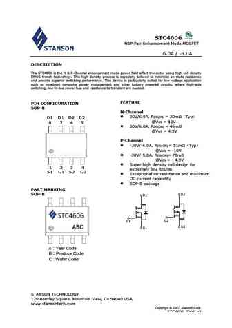
STC4606 N&P Pair Enhancement Mode MOSFET 6.0A / -6.0A DESCRIPTION The STC4606 is the N & P-Channel enhancement mode power field effect transistor using high cell density DMOS trench technology. This high density process is especially tailored to minimize on-state resistance and provide superior switching performance. This device is particularly suited for low voltage application
0.21. Size:3180K allpower
ap4606cs.pdf
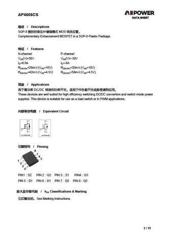
AP4606CS / Descriptions SOP-8 MOS Complementary Enhancement MOSFET in a SOP-8 Plastic Package. / Features N-channel P-channel VDS(V)=30V VDS(V)=-30V ID=6.9A ID=-6A RDS(ON)
0.22. Size:1938K anbon
as4606bs.pdf
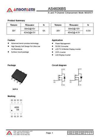
AS4606BS N and P-Channel Enhancement Mode MOSFET Product Summary V R I V R I (BR)DSS DS(on)MAX D (BR)DSS DS(on)MAX D 30m @10V 30m @-10V 30V 6A -30V -6.5A 42m @4.5V 45m @-4.5V Feature Application Advanced trench process technology Power Management High Density Cell Design For Ultra Low DC/DC Converter On-Resistance LCD TV & Monitor Display inverter
0.23. Size:361K huashuo
hsm4606.pdf
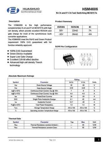
HSM4606 N-Ch and P-Ch Fast Switching MOSFETs Description Product Summary The HSM4606 is the high performance BVDSS RDSON ID complementary N-ch and P-ch MOSFETs with high 30V 22m 7A cell density, which provide excellent RDSON and gate charge for most of the synchronous buck -30V 26m -6A converter applications. The HSM4606 meet the RoHS and Green Product requirement
0.24. Size:318K cn puolop
pt4606.pdf
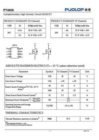
PT4606 Complementary High Density Trench MOSFET PRODUCT SUMMARY (N-Channel) PRODUCT SUMMARY (P-Channel) VDSS ID RDS(on) (m ) Max VDSS ID RDS(on) (m ) Max 6.5A 28 @ VGS= 10V -6A 37 @ VGS= -10V 30V -30V 5A 41 @ VG 4.5V -5A 57 @ VGS= -4.5V S= D 1 D 2 SOP-8 S1 1 8 D1 2 G 1 7 D1 3 6 S 2 D2 4 5 G 2 D 2 S 1 S 2 ABSOLUTE MAXIMUM RATINGS (TA = 25 C unless otherwise noted) Param
0.25. Size:948K cn super semi
sgo4606t.pdf
SUPER-SEMI SUPER-MOSFET Super Gate Metal Oxide Semiconductor Field Effect Transistor 30V Complementary Power Transistor SGO4606T Rev. 1.0 Aug. 2016 www.supersemi.com.cn Jun, 2015 SG-FET SGO4606T 30V Complementary MOSFET Description Features The SG-MOSFET uses trench MOSFET technology that is N-Channel P-Channel uniquely optimized to provide the most efficient h
0.26. Size:3139K winsok
wsp4606a.pdf
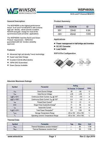
WSP4606A N-Ch and P-Channel MOSFET General Description Product Summery The WSP4606A is the highest performance BVDSS RDSON ID trench N-ch and P-ch MOSFETs with extreme high cell density , which provide excellent 30V 22m 6.8A RDSON and gate charge for most of the synchronous buck converter applications . -5.6A -30V 45m The WSP4606A meet the RoHS and Green Applications
0.27. Size:1338K winsok
wsp4606.pdf
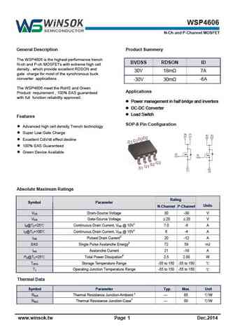
WSP4606 N-Ch and P-Channel MOSFET General Description Product Summery The WSP4606 is the highest performance trench BVDSS RDSON ID N-ch and P-ch MOSFETs with extreme high cell density , which provide excellent RDSON and 30V 18m 7A gate charge for most of the synchronous buck converter applications . -6A -30V 30m The WSP4606 meet the RoHS and Green Applications Produc
0.28. Size:493K cn sino-ic
se4606l.pdf
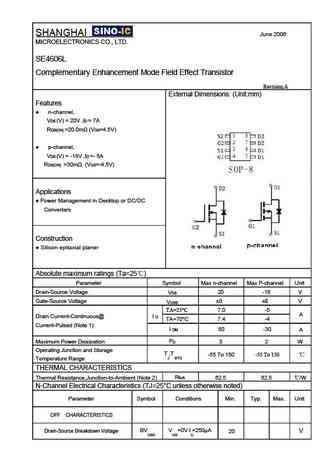
SHANGHAI June 2006 MICROELECTRONICS CO., LTD. SE4606L Complementary Enhancement Mode Field Effect Transistor Revision A External Dimensions (Unit mm) Features n-channel, VDS (V) = 20V ,ID =7A RDS(ON) =20.0m (VGS=4.5V) p-channel, VDS (V) = -18V ,ID =- 5A RDS(ON) =30m (VGS=-4.5V) Applications Power Management in Desktop or DC/DC Converters Construction Sili
0.29. Size:428K cn sino-ic
se4606s.pdf
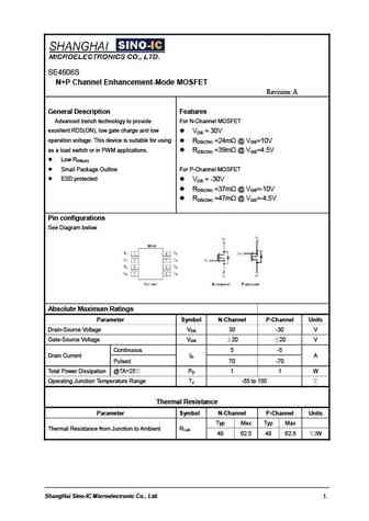
SE4606S N+P Channel Enhancement-Mode MOSFET Revision A General Description Features Advanced trench technology to provide For N-Channel MOSFET excellent RDS(ON), low gate charge and low VDS = 30V operation voltage. This device is suitable for using RDS(ON) =24m @ VGS=10V as a load switch or in PWM applications. RDS(ON) =39m @ VGS=4.5V Low RDS(on)
0.30. Size:385K cn sino-ic
se4606.pdf
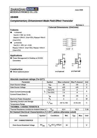
SHANGHAI June 2006 MICROELECTRONICS CO., LTD. SE4606 Complementary Enhancement Mode Field Effect Transistor Revision A External Dimensions (Unit mm) Features n-channel, VDS (V) = 30V ,ID = 8.5A RDS(ON)
0.31. Size:25275K cn sps
sm4606.pdf
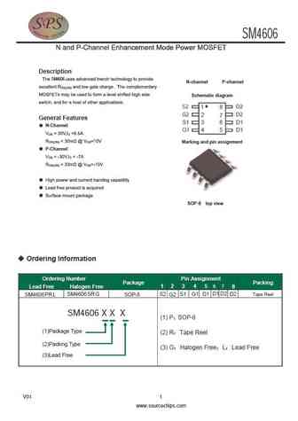
SM4606 P-Channel Enhancement-Mode MOSFET Description SM4606 N-channel P-channel Schematic diagram General Features N-Channel Marking and pin assignment P-Channel SOP-8 top view Ordering Information Ordering Number Pin Assignment Package Packing 1 2 3 4 5 6 7 Lead Free Halogen Free 8 SM4606SR G D1 D2 SM4606PR L SOP-8 S2 S1 G1 D1 D2 G2 Tape Reel SM4606
0.32. Size:2360K cn vbsemi
vbza4606.pdf
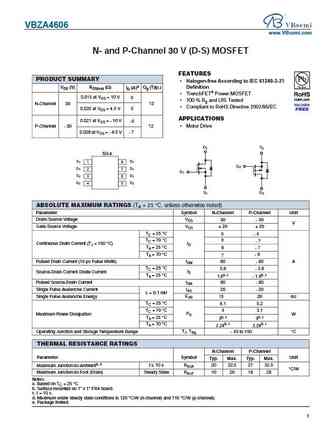
VBZA4606 www.VBsemi.com N- and P-Channel 30 V (D-S) MOSFET FEATURES PRODUCT SUMMARY Halogen-free According to IEC 61249-2-21 VDS (V) RDS(on) ( ) Definition ID (A)a Qg (Typ.) TrenchFET Power MOSFET 0.015 at VGS = 10 V 9 100 % Rg and UIS Tested N-Channel 30 13 Compliant to RoHS Directive 2002/95/EC 0.020 at VGS = 4.5 V 8 APPLICATIONS 0.021 at VGS = - 10 V - 8
0.33. Size:967K cn vbsemi
mt4606.pdf

MT4606 www.VBsemi.tw N- and P-Channel 30 V (D-S) MOSFET FEATURES PRODUCT SUMMARY Halogen-free According to IEC 61249-2-21 VDS (V) RDS(on) ( ) Definition ID (A)a Qg (Typ.) TrenchFET Power MOSFET 0.018 at VGS = 10 V 8e 100 % Rg and UIS Tested N-Channel 30 0.020 at VGS = 8 V 8e 6.2 Compliant to RoHS Directive 2002/95/EC 0.024 at VGS = 4.5 V 8e 0.032 at VGS =
0.34. Size:1506K cn vbsemi
nce4606.pdf
NCE4606 www.VBsemi.tw N- and P-Channel 30 V (D-S) MOSFET FEATURES PRODUCT SUMMARY Halogen-free According to IEC 61249-2-21 VDS (V) RDS(on) ( ) Definition ID (A)a Qg (Typ.) TrenchFET Power MOSFET 0.018 at VGS = 10 V 8e 100 % Rg and UIS Tested N-Channel 30 0.020 at VGS = 8 V 8e 6.2 Compliant to RoHS Directive 2002/95/EC 0.024 at VGS = 4.5 V 8e 0.032 at VGS
0.35. Size:963K cn vbsemi
ao4606a.pdf

AO4606A www.VBsemi.tw N- and P-Channel 30 V (D-S) MOSFET FEATURES PRODUCT SUMMARY Halogen-free According to IEC 61249-2-21 VDS (V) RDS(on) ( ) Definition ID (A)a Qg (Typ.) TrenchFET Power MOSFET 0.018 at VGS = 10 V 8e 100 % Rg and UIS Tested N-Channel 30 0.020 at VGS = 8 V 8e 6.2 Compliant to RoHS Directive 2002/95/EC 0.024 at VGS = 4.5 V 8e 0.032 at VGS
0.36. Size:1633K cn yangzhou yangjie elec
yjs4606a.pdf
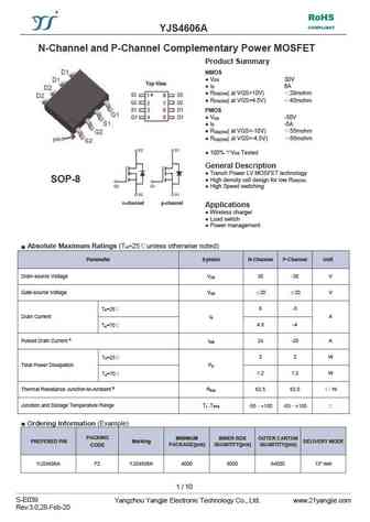
RoHS COMPLIANT YJS4606A N-Channel and P-Channel Complementary Power MOSFET Product Summary NMOS V 30V DS I 6A D R ( at VGS=10V) 29mohm DS(ON) R ( at VGS=4.5V) 40mohm DS(ON) PMOS V -30V DS I -5A D R ( at VGS=-10V) 55mohm DS(ON) R ( at VGS=-4.5V) 68mohm DS(ON) 100% V Tested DS General Description Tr
0.37. Size:1907K cn hmsemi
hm4606c.pdf
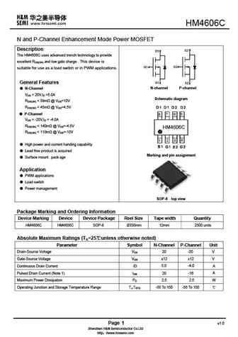
HM4606C N and P-Channel Enhancement Mode Power MOSFET Description The HM4606C uses advanced trench technology to provide excellent RDS(ON) and low gate charge . This device is suitable for use as a load switch or in PWM applications. General Features N-channel P-channel N-Channel VDS = 20V,ID =5.0A Schematic diagram RDS(ON)
0.38. Size:679K cn hmsemi
hm4606d.pdf

HM4606D N and P-Channel Enhancement Mode Power MOSFET Description The HM4606D uses advanced trench technology to provide excellent RDS(ON) and low gate charge . This device is suitable for use as a load switch or in PWM applications. General Features N-channel P-channel N-Channel VDS = 30V,ID =6.5A Schematic diagram RDS(ON)
0.39. Size:922K cn hmsemi
hm4606b.pdf

HM4606B N and P-Channel Enhancement Mode Power MOSFET Description The HM4606B uses advanced trench technology to provide excellent RDS(ON) and low gate charge . The complementary MOSFETs may be used to form a level shifted high side switch, and for a host of other applications. General Features N-channel P-channel N-Channel VDS = 30V,ID =6.5A Schematic diagram RDS(ON)
0.40. Size:1544K cn hmsemi
hm4606.pdf
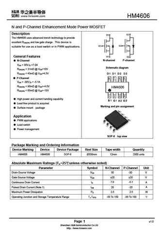
HM4606 N and P-Channel Enhancement Mode Power MOSFET Description The HM4606 uses advanced trench technology to provide excellent RDS(ON) and low gate charge . This device is suitable for use as a load switch or in PWM applications. General Features N-channel P-channel N-Channel VDS = 30V,ID =7.0A Schematic diagram RDS(ON)
0.41. Size:813K cn hmsemi
hm4606a.pdf
HM4606A N and P-Channel Enhancement Mode Power MOSFET Description The HM4606A uses advanced trench technology to provide excellent RDS(ON) and low gate charge . The complementary MOSFETs may be used to form a level shifted high side switch, and for a host of other applications. General Features N-channel P-channel N-Channel VDS = 30V,ID =6.5A Schematic diagram RDS(ON)
0.42. Size:1959K cn apm
ap4606c.pdf
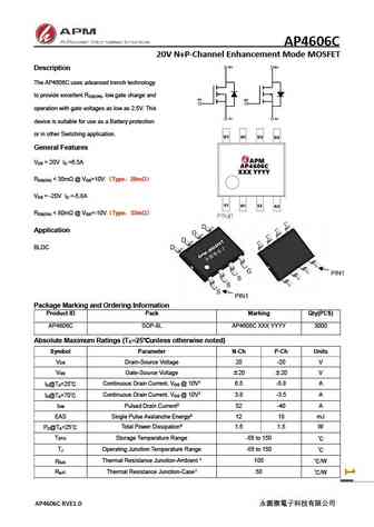
AP4606C 20V N+P-Channel Enhancement Mode MOSFET Description The AP4606C uses advanced trench technology to provide excellent R , low gate charge and DS(ON) operation with gate voltages as low as 2.5V. This device is suitable for use as a Battery protection or in other Switching application. General Features V = 20V I =6.5A DS D R
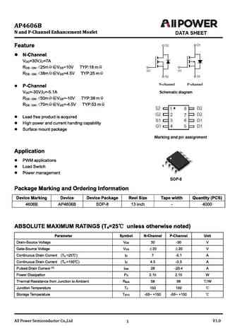
0.43. Size:1979K cn apm
ap4606b.pdf
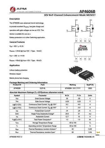
AP4606B 30V N+P-Channel Enhancement Mode MOSFET Description The AP4606B uses advanced trench technology to provide excellent R , low gate charge and DS(ON) operation with gate voltages as low as 4.5V. This device is suitable for use as a Battery protection or in other Switching application. General Features V = 30V I =6.2A DS D R
Otros transistores... 4401
, 4402
, 4407
, 4409
, 4410
, 4435
, 4501
, 4542
, IRF4905
, 4611
, 4612
, 4616
, 4622
, 4803
, 4812
, 4835
, 4920
.