80N03 MOSFET Equivalente. Reemplazo. Hoja de especificaciones. Principales características
Número de Parte: 80N03
Tipo de FET: MOSFET
Polaridad de transistor: N
ESPECIFICACIONES MÁXIMAS
Pdⓘ - Máxima disipación de potencia: 83 W
|Vds|ⓘ - Voltaje máximo drenador-fuente: 30 V
|Vgs|ⓘ - Voltaje máximo fuente-puerta: 20 V
|Id|ⓘ - Corriente continua de drenaje: 80 A
Tjⓘ - Temperatura máxima de unión: 175 °C
CARACTERÍSTICAS ELÉCTRICAS
Cossⓘ - Capacitancia de salida: 460 pF
RDSonⓘ - Resistencia estado encendido drenaje a fuente: 0.006 Ohm
Búsqueda de reemplazo de 80N03 MOSFET
- Selecciónⓘ de transistores por parámetros
80N03 datasheet
80n03.pdf
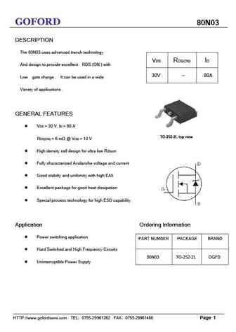
GOFORD 80N03 DESCRIPTION The 80N03 uses advanced trench technology VDS RDS(ON) ID And design to provide excellent RDS (ON ) with 30V -- 80A Low gate charge . It can be used in a wide Vanety of applications . GENERAL FEATURES VDS = 30 V, ID = 80 A TO-252-2L top view RDS(ON)
80n03 dfn.pdf
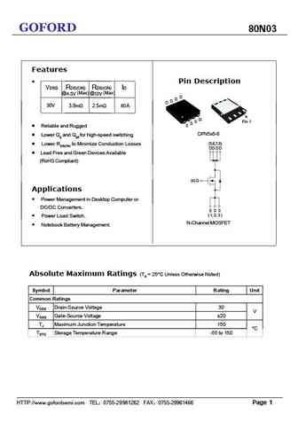
GOFORD 80N03 Features Pin Description VDSS RDS(ON) RDS(ON) ID @4.5V (Max) @10V (Max) D D D D 30V 3.9m 2.5m 80 A G Pin 1 S S Reliable and Rugged S DFN5x6-8 Lower Qg and Qgd for high-speed switching (5,6,7,8) Lower RDS(ON) to Minimize Conduction Losses DDDD Lead Free and Green Devices Available (RoHS Compliant) (4) G Applications Power Management in
msk80n03nf.pdf
www.msksemi.com MSK80N03NF Semiconductor Compiance Description The uses advanced trench technology MSK80N03NF and design to provide excellent RDS(ON) with low D D D D gatecharge. It can be used in a wide variety of applications. General Features VDS=30V,ID=80A S S S G RDS(ON)
stp80n03l-06.pdf
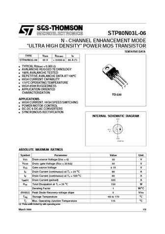
STP80N03L-06 N - CHANNEL ENHANCEMENT MODE "ULTRA HIGH DENSITY" POWER MOS TRANSISTOR TENTATIVE DATA TYPE V R I DSS DS(on) D STP80N03L-06 30 V
np80n03cde np80n03dde np80n03ede np80n03kde np80n03mde np80n03nde.pdf
To our customers, Old Company Name in Catalogs and Other Documents On April 1st, 2010, NEC Electronics Corporation merged with Renesas Technology Corporation, and Renesas Electronics Corporation took over all the business of both companies. Therefore, although the old company name remains in this document, it is a valid Renesas Electronics document. We appreciate your understanding.
np80n03cle np80n03dle np80n03ele np80n03kle np80n03mle np80n03nle.pdf
To our customers, Old Company Name in Catalogs and Other Documents On April 1st, 2010, NEC Electronics Corporation merged with Renesas Technology Corporation, and Renesas Electronics Corporation took over all the business of both companies. Therefore, although the old company name remains in this document, it is a valid Renesas Electronics document. We appreciate your understanding.
rmw180n03.pdf
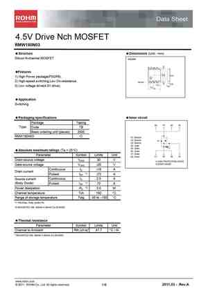
Data Sheet 4.5V Drive Nch MOSFET RMW180N03 Structure Dimensions (Unit mm) Silicon N-channel MOSFET PSOP8 (8) (7) (6) (5) Features 0 0.1 1) High Power package(PSOP8). 2) High-speed switching,Low On-resistance. 1pin mark (1) (2) (3) (4) 0.22 0.4 3) Low voltage drive(4.5V drive). 0.9 1.27 5.0 Application Switching Packaging specifications Inner circuit
rmw280n03.pdf
Data Sheet 4.5V Drive Nch MOSFET RMW280N03 Structure Dimensions (Unit mm) Silicon N-channel MOSFET PSOP8 (8) (7) (6) (5) Features 0 0.1 1) High Power package(PSOP8). 1pin mark 2) High-speed switching,Low On-resistance. (1) (2) (3) (4) 0.22 0.4 0.9 3) Low voltage drive(4.5V drive). 1.27 5.0 Application Switching Packaging specifications Inner circuit
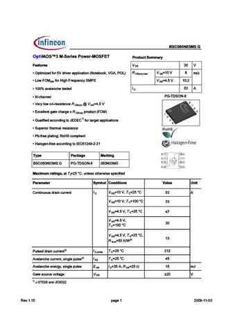
bsc080n03msg.pdf
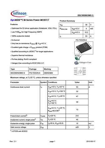
BSC080N03MS G OptiMOS 3 M-Series Power-MOSFET Product Summary Features VDS 30 V Optimized for 5V driver application (Notebook, VGA, POL) RDS(on),max VGS=10 V 8 mW Low FOMSW for High Frequency SMPS VGS=4.5 V 10.2 100% avalanche tested ID 53 A N-channel PG-TDSON-8 Very low on-resistance R @ V =4.5 V DS(on) GS Excellent gate charge x R product (FOM)
ipb180n03s4l-h0 ipb180n03s4l-h0 ds 1 0.pdf
IPB180N03S4L-H0 OptiMOS -T2 Power-Transistor Product Summary V 30 V DS R 0.95 m DS(on) I 180 A D Features N-channel - Enhancement mode PG-TO263-7-3 AEC qualified MSL1 up to 260 C peak reflow 175 C operating temperature Green package (RoHS compliant) Ultra low Rds(on) 100% Avalanche tested Type Package Marking IPB180N03S4L-H0 PG-TO263-7-3 4N
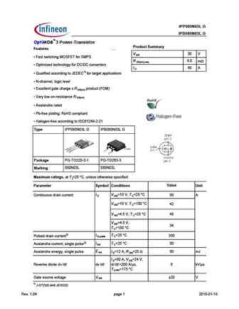
ipp080n03l .pdf
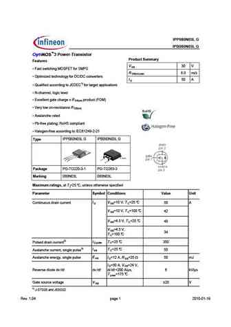
Type IPP080N03L G IPB080N03L G 3 Power-Transistor Product Summary Features V 30 V DS Fast switching MOSFET for SMPS R 8.0 mW DS(on),max Optimized technology for DC/DC converters I 50 A D Qualified according to JEDEC1) for target applications N-channel, logic level Excellent gate charge x R product (FOM) DS(on) Very low on-resistance R DS(on)
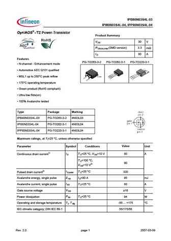
ipb80n03s4l-03 ipi80n03s4l-04 ipp80n03s4l-04.pdf
IPB80N03S4L-03 IPI80N03S4L-04, IPP80N03S4L-04 OptiMOS -T2 Power-Transistor Product Summary V 30 V DS R (SMD version) 3.3 m DS(on),max I 80 A D Features PG-TO263-3-2 PG-TO262-3-1 PG-TO220-3-1 N-channel - Enhancement mode Automotive AEC Q101 qualified MSL1 up to 260 C peak reflow 175 C operating temperature Green product (RoHS compliant) Ultra low
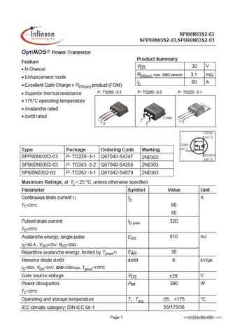
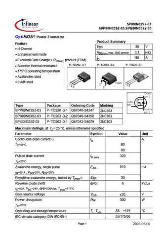
spi80n03s2-03 spp80n03s2-03 spb80n03s2-03.pdf
www.DataSheet4U.com SPI80N03S2-03 SPP80N03S2-03,SPB80N03S2-03 OptiMOS Power-Transistor Product Summary Feature VDS 30 V N-Channel RDS(on) max. SMD version 3.1 m Enhancement mode ID 80 A Excellent Gate Charge x RDS(on) product (FOM) P- TO262 -3-1 P- TO263 -3-2 P- TO220 -3-1 Superior thermal resistance 175 C operating temperature Avalanche rated
ipb080n03l.pdf
Type IPP080N03L G IPB080N03L G 3 Power-Transistor Product Summary Features V 30 V DS Fast switching MOSFET for SMPS R 8.0 mW DS(on),max Optimized technology for DC/DC converters I 50 A D Qualified according to JEDEC1) for target applications N-channel, logic level Excellent gate charge x R product (FOM) DS(on) Very low on-resistance R DS(on)
ipb80n03s4l-02 ipi80n03s4l-03 ipp80n03s4l-03 ipb80n03s4l-02 ipp i80n03s4l 03 ds.pdf
IPB80N03S4L-02 IPI80N03S4L-03, IPP80N03S4L-03 OptiMOS -T2 Power-Transistor Product Summary V 30 V DS R (SMD version) 2.4 m DS(on),max I 80 A D Features PG-TO263-3-2 PG-TO262-3-1 PG-TO220-3-1 N-channel - Enhancement mode Automotive AEC Q101 qualified MSL1 up to 260 C peak reflow 175 C operating temperature Green product (RoHS compliant) Ultra low
bsc080n03msg5.pdf
% ! % D %0 S 07DK >AI A@ D7E;EF3@57 0 D n) G S J57>>7@F 93F7 5 3D97 J BDA6G5F !* ( D n) 1) S , G3>;8;76 355AD6;@9 FA % 8AD F3D97F 3BB>;53F;A@E S .GB7D;AD F 7D?3
ipp080n03l.pdf
Type IPP080N03L G IPB080N03L G OptiMOS 3 Power-Transistor Product Summary Features . V 30 V DS Fast switching MOSFET for SMPS R 8.0 m DS(on),max Optimized technology for DC/DC converters I 50 A D Qualified according to JEDEC1) for target applications N-channel, logic level Excellent gate charge x R product (FOM) DS(on) Very low on-resistance R
ipi80n03s4l-03 ipp80n03s4l-03.pdf
IPB80N03S4L-02 IPI80N03S4L-03, IPP80N03S4L-03 OptiMOS -T2 Power-Transistor Product Summary V 30 V DS R (SMD version) 2.4 m DS(on),max I 80 A D Features PG-TO263-3-2 PG-TO262-3-1 PG-TO220-3-1 N-channel - Enhancement mode Automotive AEC Q101 qualified MSL1 up to 260 C peak reflow 175 C operating temperature Green product (RoHS compliant) Ultra low
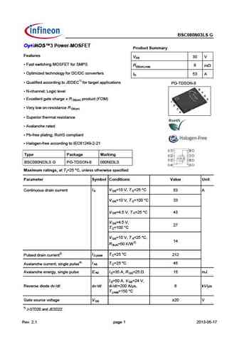
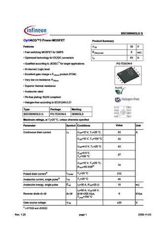
bsc080n03lsg.pdf
BSC080N03LS G OptiMOS 3 Power-MOSFET Product Summary Features VDS 30 V Fast switching MOSFET for SMPS RDS(on),max 8 mW Optimized technology for DC/DC converters ID 53 A Qualified according to JEDEC1) for target applications PG-TDSON-8 N-channel; Logic level Excellent gate charge x R product (FOM) DS(on) Very low on-resistance R DS(on) Superio
spb80n03s2.pdf
SPI80N03S2-03 SPP80N03S2-03,SPB80N03S2-03 OptiMOS Power-Transistor Product Summary Feature VDS 30 V N-Channel RDS(on) max. SMD version 3.1 m Enhancement mode ID 80 A Excellent Gate Charge x RDS(on) product (FOM) P- TO262 -3-1 P- TO263 -3-2 P- TO220 -3-1 Superior thermal resistance 175 C operating temperature Avalanche rated dv/dt rated Type Pa
bsc080n03ms.pdf
BSC080N03MS G OptiMOS 3 M-Series Power-MOSFET Product Summary Features VDS 30 V Optimized for 5V driver application (Notebook, VGA, POL) RDS(on),max VGS=10 V 8 mW Low FOMSW for High Frequency SMPS VGS=4.5 V 10.2 100% avalanche tested ID 53 A N-channel PG-TDSON-8 Very low on-resistance R @ V =4.5 V DS(on) GS Excellent gate charge x R product (FOM)
bsc080n03ls.pdf
BSC080N03LS G OptiMOS 3 Power-MOSFET Product Summary Features VDS 30 V Fast switching MOSFET for SMPS RDS(on),max 8 mW Optimized technology for DC/DC converters ID 53 A Qualified according to JEDEC1) for target applications PG-TDSON-8 N-channel; Logic level Excellent gate charge x R product (FOM) DS(on) Very low on-resistance R DS(on) Superio
bsc080n03ls5.pdf
& " & E $;B1= !#& ' $=;0@/? &@99-=D Features D Q 2CD CG D49 ?8 ') - . 7@B -'*- m D n) m x Q ) AD > J65 D649?@=@8I 7@B 4@?F6BD6BC D 1) Q + E2= 7 65 244@B5 ?8 D@ $ 7@B D2B86D 2AA= 42D @?C G D ON Q ( 492??6= &@8 4 =6F6= Q H46==6?D 82D6 492B86 H AB@5E4D ) ' D n) Q /6BI =@G @? B6C CD2?46 D n) Q -EA6B @B D96B>2= B6C CD2?46 Q F2=2?496 B2D65 Q *3 7B66 A=2D ?8 , @"- 4
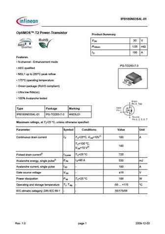
ipb180n03s4l-01 ipb180n03s4l-01 ds 1 0.pdf
IPB180N03S4L-01 OptiMOS -T2 Power-Transistor Product Summary V 30 V DS R 1.05 m DS(on) I 180 A D Features N-channel - Enhancement mode PG-TO263-7-3 AEC qualified MSL1 up to 260 C peak reflow 175 C operating temperature Green package (RoHS compliant) Ultra low Rds(on) 100% Avalanche tested Type Package Marking IPB180N03S4L-01 PG-TO263-7-3 4N
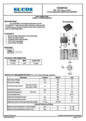
ssd80n03.pdf
SSD80N03 80A , 30V , RDS(ON) 5.5m N-Ch Enhancement Mode Power MOSFET Elektronische Bauelemente RoHS Compliant Product A suffix of -C specifies halogen free DESCRIPTION TO-252(D-Pack) The SSD80N03 is the highest performance trench N-ch MOSFETs with extreme high cell density , which provide excellent RDS(ON) and gate charge for most of the synchronous buck converter
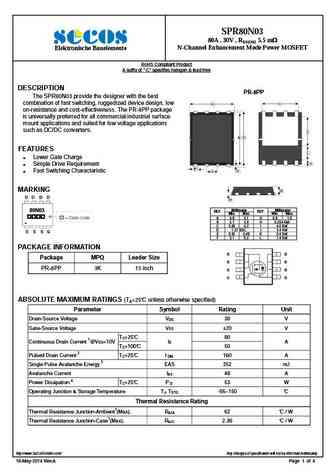
spr80n03.pdf
SPR80N03 80A , 30V , RDS(ON) 5.5 m N-Channel Enhancement Mode Power MOSFET Elektronische Bauelemente RoHS Compliant Product A suffix of -C specifies halogen & lead-free DESCRIPTION PR-8PP The SPR80N03 provide the designer with the best combination of fast switching, ruggedized device design, low on-resistance and cost-effectiveness. The PR-8PP package
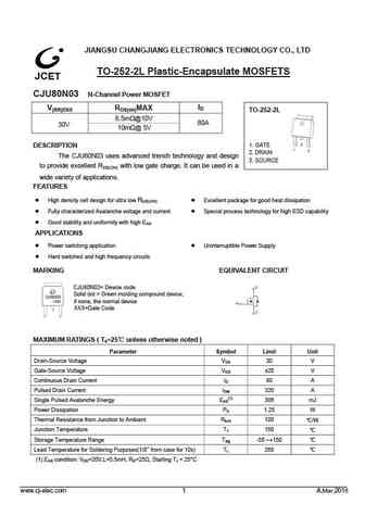
cju80n03.pdf
JIANGSU CHANGJIANG ELECTRONICS TECHNOLOGY CO., LTD TO-252-2L Plastic-Encapsulate MOSFETS CJU80N03 N-Channel Power MOSFET ID V(BR)DSS R DS(on) MAX TO-252-2L 6.5m @10V 80A 30V 10m @ 5 V 1. GATE DESCRIPTION 2. DRAIN The CJU80N03 uses advanced trench technology and design 3. SOURCE to provide excellent RDS(ON) with low gate charge. It can be used in a wide varie
ap80n03gp.pdf
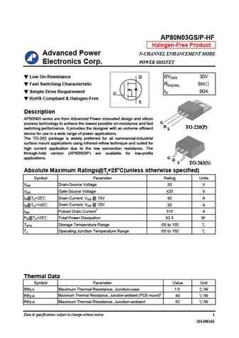
AP80N03GS/P-HF Halogen-Free Product Advanced Power N-CHANNEL ENHANCEMENT MODE Electronics Corp. POWER MOSFET Low On-Resistance BVDSS 30V D Fast Switching Characteristic RDS(ON) 8m Simple Drive Requirement ID 80A G RoHS Compliant & Halogen-Free S Description AP80N03 series are from Advanced Power innovated design and silicon G process technology to achieve the low
am80n03-06d.pdf
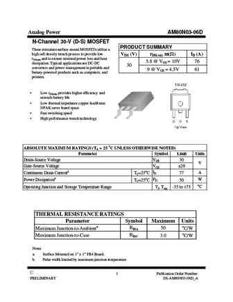
Analog Power AM80N03-06D N-Channel 30-V (D-S) MOSFET PRODUCT SUMMARY These miniature surface mount MOSFETs utilize a high cell density trench process to provide low VDS (V) rDS(on) m( ) ID (A) rDS(on) and to ensure minimal power loss and heat 5.8 @ VGS = 10V 76 dissipation. Typical applications are DC-DC 30 converters and power management in portable and 9 @ VGS = 4.5V 61 batte
am80n03-05d.pdf
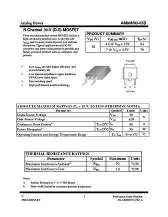
Analog Power AM80N03-05D N-Channel 30-V (D-S) MOSFET PRODUCT SUMMARY These miniature surface mount MOSFETs utilize a high cell density trench process to provide low VDS (V) rDS(on) m( ) ID (A) rDS(on) and to ensure minimal power loss and heat 4.8 @ VGS = 10V 84 dissipation. Typical applications are DC-DC 30 converters and power management in portable and 7 @ VGS = 4.5V 70 batte
brcs080n03yb.pdf
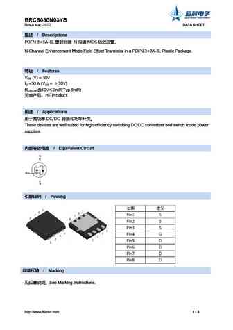
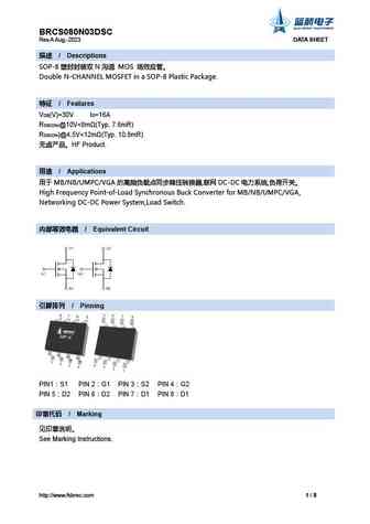
BRCS080N03YB Rev.A Mar.-2022 DATA SHEET / Descriptions PDFN 3 3A-8L N MOS N-Channel Enhancement Mode Field Effect Transistor in a PDFN 3 3A-8L Plastic Package. / Features VDS (V) = 30V ID =30 A (VGS = 20V) RDS(ON)@10V 9mR(Typ.8mR) HF Product. / Applications DC/DC
brcs80n03dp.pdf
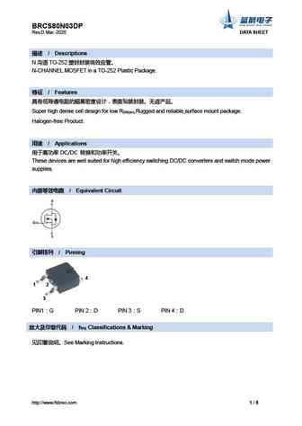
BRCS80N03DP Rev.D Mar.-2020 DATA SHEET / Descriptions N TO-252 N-CHANNEL MOSFET in a TO-252 Plastic Package. / Features Super high dense cell design for low RDS(on),Rugged and reliable,surface mount package. Halogen-free Product. / Applicati
ftk80n03d.pdf
SEMICONDUCTOR FTK80N03D TECHNICAL DATA N-Channel Power MOSFET A I C J GENERAL DESCRIPTION The FTK80N03D uses advanced trench technology and design to DIM MILLIMETERS A 6 50 0 2 provide excellent RDS(ON) with low gate charge. B 5 60 0 2 C 5 20 0 2 It can be used in awide variety of applications. D 1 50 0 2 E 2 70 0 2 F 2 30 0 1 H H 1 00 MAX I 2 30 0
dhd80n03.pdf
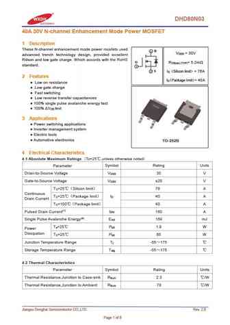
DHD80N03 40A 30V N-channel Enhancement Mode Power MOSFET 1 Description These N-channel enhancement mode power mosfets used 2 D V = 30V DSS advanced trench technology design, provided excellent Rdson and low gate charge. Which accords with the RoHS G R = 5.2m DS(on) (TYP) standard. 1 3 S I Silicon limit = 76A D 2 Features I Package limit 40A = D Low on resis
msd80n03.pdf
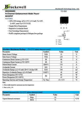
Bruckewell Technology Corp., Ltd. MSD80N03 N-Channel Enhancement Mode Power MOSFET FEATURES 100% UIS testing, @VD=15V, L=0.1mH, VG=10V, IL=40V, rated VDS=25V N-CH Simple Drive Requirement Repetitive Avalanche Rated Fast Switching Characteristic RoHS compliant package & Halogen-free package Absolute Maximum Ratings (Tc=25 C unless otherwise noted) Pa
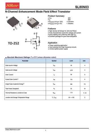
sl80n03.pdf
SL80N03 N-Channel Enhancement Mode Field Effect Transistor Product Summary V 30V DS I 80A D R ( at V = 10V) 6.5mohm DS(ON) GS R ( at V = 5V) 10mohm DS(ON) GS Features High density cell design for ultra low Rdson Fully characterized avalanche voltage and current Good stability and uniformity with high EAS Excellent package for good heat dissi
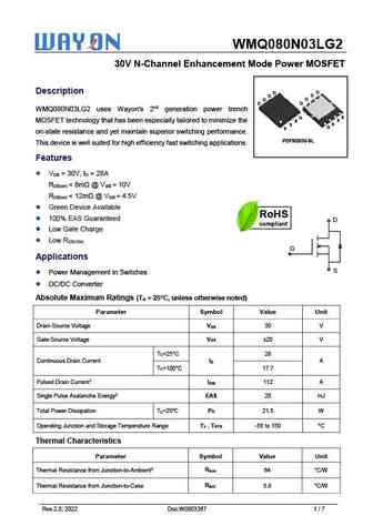
wmq080n03lg2.pdf
WMQ080N03LG2 30V N-Channel Enhancement Mode Power MOSFET Description D D D D D D D D WMQ080N03LG2 uses Wayon's 2nd generation power trench S G S MOSFET technology that has been especially tailored to minimize the S S S G S on-state resistance and yet maintain superior switching performance. PDFN3030-8L This device is well suited for high efficiency fast switching appl
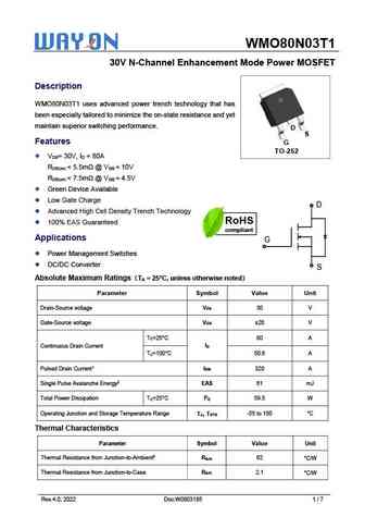
wmo80n03t1.pdf
WMO80N03T1 30V N-Channel Enhancement Mode Power MOSFET Description WMO80N03T1 uses advanced power trench technology that has been especially tailored to minimize the on-state resistance and yet maintain superior switching performance. D S Features G TO-252 V = 30V, I = 80A DS D R
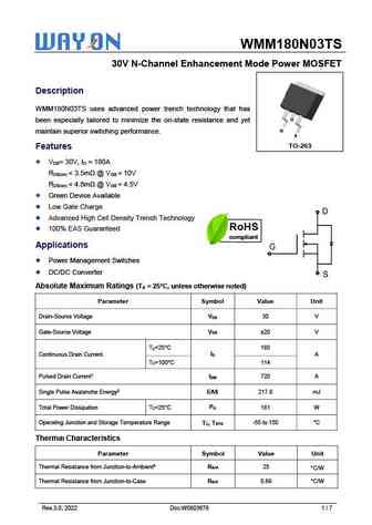
wmm180n03ts.pdf
WMM180N03TS 30V N-Channel Enhancement Mode Power MOSFET Description WMM180N03TS uses advanced power trench technology that has D been especially tailored to minimize the on-state resistance and yet G maintain superior switching performance. S TO-263 Features V = 30V, I = 180A DS D R
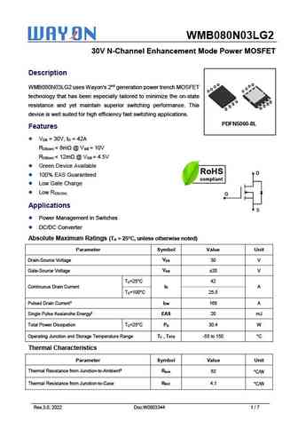
wmb080n03lg2.pdf
WMB080N03LG2 30V N-Channel Enhancement Mode Power MOSFET Description D D D D WMB080N03LG2 uses Wayon's 2nd generation power trench MOSFET D D D D technology that has been especially tailored to minimize the on-state G ss resistance and yet maintain superior switching performance. This s ss G s device is well suited for high efficiency fast switching applications. PDFN5
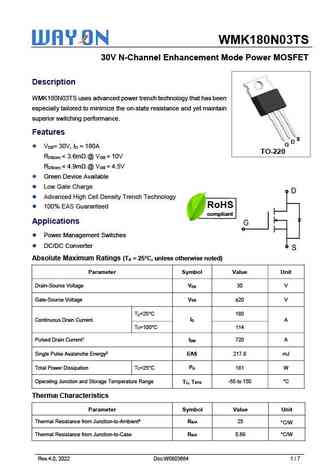
wmk180n03ts.pdf
WMK180N03TS 30V N-Channel Enhancement Mode Power MOSFET Description WMK180N03TS uses advanced power trench technology that has been especially tailored to minimize the on-state resistance and yet maintain superior switching performance. Features S D G V = 30V, I = 180A DS D TO-220 R
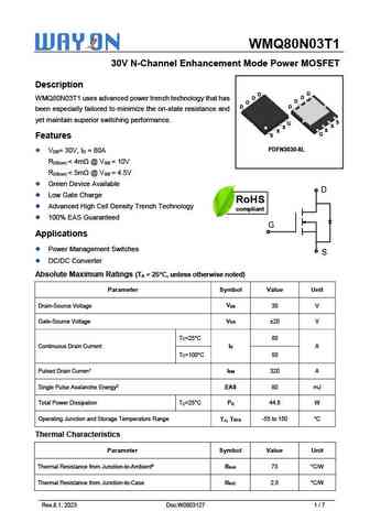
wmq80n03t1.pdf
WMQ80N03T1 30V N-Channel Enhancement Mode Power MOSFET Description D D D WMQ80N03T1 uses advanced power trench technology that has D D D D D been especially tailored to minimize the on-state resistance and yet maintain superior switching performance. S G S S S S G S Features PDFN3030-8L V = 30V, I = 80A DS D R
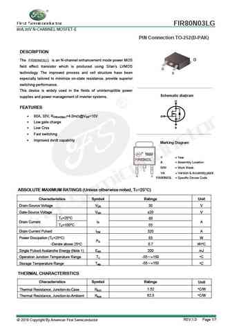
fir80n03lg.pdf
FIR80N03LG 80A,30V N-CHANNEL MOSFET-E PIN Connection TO-252(D-PAK) DESCRIPTION D The is an N-channel enhancement mode power MOS FIR80N03LG field effect transistor which is produced using Silan's LVMOS G technology. The improved process and cell structure have been S especially tailored to minimize on-state resistance, provide superior switching performance. This device is w
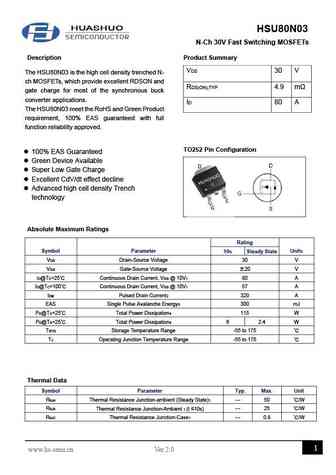
hsu80n03.pdf
HSU80N03 N-Ch 30V Fast Switching MOSFETs Description Product Summary VDS 30 V The HSU80N03 is the high cell density trenched N- ch MOSFETs, which provide excellent RDSON and RDS(ON),TYP 4.9 m gate charge for most of the synchronous buck converter applications. ID 80 A The HSU80N03 meet the RoHS and Green Product requirement, 100% EAS guaranteed with full function reliab
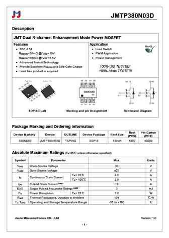
jmtp380n03d.pdf
JMTP380N03D Description JMT Dual N-channel Enhancement Mode Power MOSFET Features Application 30V, 4.5A Load Switch R
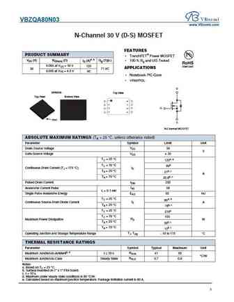
vbzqa80n03.pdf
VBZQA80N03 www.VBsemi.com N-Channel 30 V (D-S) MOSFET FEATURES PRODUCT SUMMARY TrenchFET Power MOSFET VDS (V) RDS(on) ( ) ID (A)a, e Qg (Typ.) 100 % Rg and UIS Tested 0.003 at VGS = 10 V 120 APPLICATIONS 30 71 nC 0.005 at VGS = 4.5 V 90 Notebook PC Core VRM/POL D DFN5X6 Top View Top View Bottom View 1 8 2 7 3 6 G 4 5 PIN1 S N-Channel MOSFET
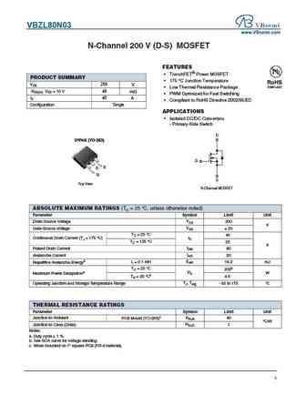
vbzl80n03.pdf
VBZL80N03 www.VBsemi.com N-Channel 200 V (D-S) MOSFET FEATURES TrenchFET Power MOSFET PRODUCT SUMMARY 175 C Junction Temperature 200 VDS V Low Thermal Resistance Package RDS(on) VGS = 10 V 48 m PWM Optimized for Fast Switching ID 40 A Compliant to RoHS Directive 2002/95/EC Configuration Single APPLICATIONS Isolated DC/DC Converters - Primary-Si
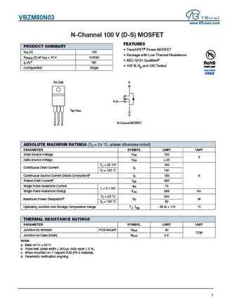
vbzm80n03.pdf
VBZM80N03 www.VBsemi.com N-Channel 100 V (D-S) MOSFET FEATURES PRODUCT SUMMARY TrenchFET Power MOSFET VDS (V) 100 Package with Low Thermal Resistance RDS(on) ( ) at VGS = 10 V 0.0038 AEC-Q101 Qualifiedd ID (A) a 180 100 % Rg and UIS Tested Configuration Single D TO-220 G Top View S N-Channel MOSFET G D S ABSOLUTE MAXIMUM RATINGS (TC = 25 C, unless other
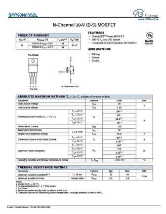
spp80n03s2l.pdf
SPP80N03S2L www.VBsemi.tw N-Channel 30-V (D-S) MOSFET FEATURES PRODUCT SUMMARY TrenchFET Power MOSFET VDS (V) RDS(on) ( ) ID (A)a, e Qg (Typ) 100 % Rg and UIS Tested Compliant to RoHS Directive 2011/65/EU 0.0035 at VGS = 10 V 98 30 82 nC 0.0045 at VGS = 4.5 V 98 APPLICATIONS OR-ing TO-220AB D Server DC/DC G S G D S N-Channel MOSFET Top View
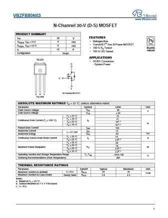
vbzfb80n03.pdf
VBZFB80N03 www.VBsemi.com N-Channel 30-V (D-S) MOSFET PRODUCT SUMMARY FEATURES VDS 30 V Halogen-free 6 RDS(on) VGS = 10 V m TrenchFET Gen III Power MOSFET RDS(on) VGS = 4.5 V 8 m 100 % Rg Tested RoHS ID 70 A COMPLIANT 100 % UIS Tested Configuration Single APPLICATIONS TO-251 DC/DC Conversion D - System Power G S N-Channel MOSFET G D S
vbze80n03.pdf
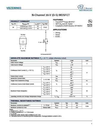
VBZE80N03 www.VBsemi.com N-Channel 30-V (D-S) MOSFET FEATURES PRODUCT SUMMARY TrenchFET Power MOSFET VDS (V) RDS(on) ( ) ID (A)a, e Qg (Typ) 100 % Rg and UIS Tested Compliant to RoHS Directive 2011/65/EU 0.007at VGS = 10 V 85 33 nC 30 0.011 at VGS = 4.5 V 50 APPLICATIONS D OR-ing TO-252 Server DC/DC G G D S Top View S N-Channel MOSFET ABSO
yjd80n03a.pdf
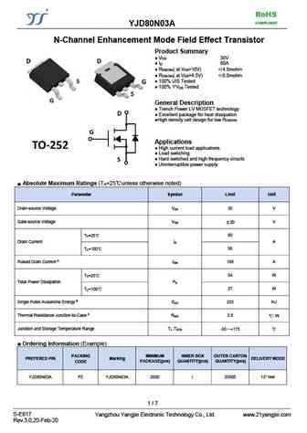
RoHS COMPLIANT YJD80N03A N-Channel Enhancement Mode Field Effect Transistor Product Summary V 30V DS I 80A D R ( at V =10V) 4.5mohm DS(ON) GS R ( at V =4.5V) 6.0mohm DS(ON) GS 100% UIS Tested 100% V Tested DS General Description Trench Power LV MOSFET technology Excellent package for heat dissipation High density cell
yjd80n03b.pdf
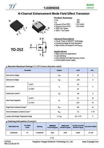
RoHS COMPLIANT YJD80N03B N-Channel Enhancement Mode Field Effect Transistor Product Summary V 30V DS I 80A D R ( at V =10V) 5.5 mohm DS(ON) GS R ( at V =4.5V) 8.0 mohm DS(ON) GS 100% UIS Tested 100% VDS Tested General Description Trench Power LV MOSFET technology Excellent package for heat dissipation High density cel
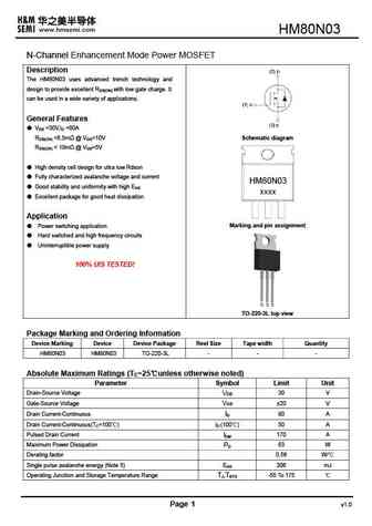
hm80n03i.pdf
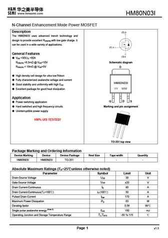
HM80N03I N-Channel Enhancement Mode Power MOSFET Description The HM80N03I uses advanced trench technology and design to provide excellent RDS(ON) with low gate charge. It can be used in a wide variety of applications. General Features VDS =30V,ID =80A RDS(ON)
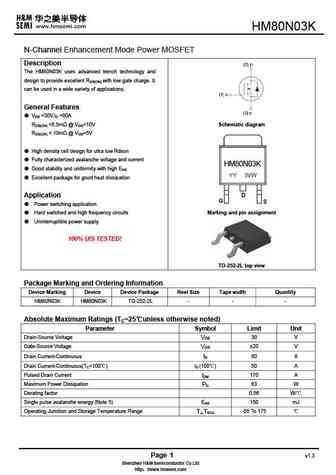
hm80n03k.pdf
N-Channel Enhancement Mode Power MOSFET Description The uses advanced trench technology and design to provide excellent RDS(ON) with low gate charge. It can be used in a wide variety of applications. General Features VDS =30V,ID =80A RDS(ON)
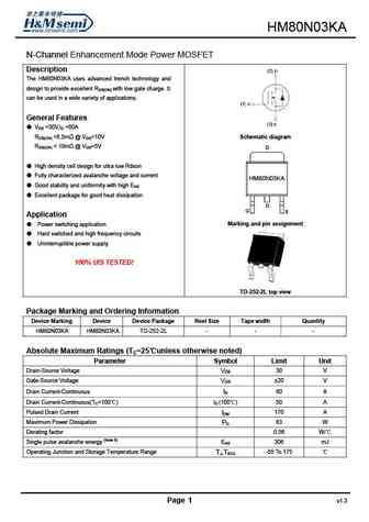
hm80n03ka.pdf
HM80N03KA N-Channel Enhancement Mode Power MOSFET Description The HM80N03KA uses advanced trench technology and design to provide excellent RDS(ON) with low gate charge. It can be used in a wide variety of applications. General Features VDS =30V,ID =80A RDS(ON)
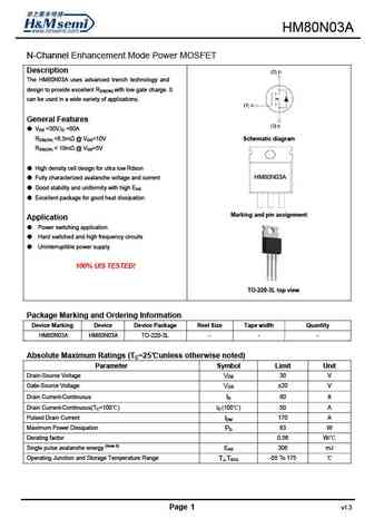
hm80n03a.pdf
HM80N03A N-Channel Enhancement Mode Power MOSFET Description The HM80N03A uses advanced trench technology and design to provide excellent RDS(ON) with low gate charge. It can be used in a wide variety of applications. General Features VDS =30V,ID =80A RDS(ON)
ipb080n03l.pdf
isc N-Channel MOSFET Transistor IPB080N03L DESCRIPTION Drain Current I = 50A@ T =25 D C Drain Source Voltage V = 30V(Min) DSS 100% avalanche tested Minimum Lot-to-Lot variations for robust device performance and reliable operation APPLICATIONS . Designed for high current, high speed switching, switch mode power supplies. ABSOLUTE MAXIMUM RATINGS(T =25 ) C SY
ipp080n03l.pdf
INCHANGE Semiconductor isc N-Channel MOSFET Transistor IPP080N03L IIPP080N03L FEATURES Static drain-source on-resistance RDS(on) 8.0m Enhancement mode Vth =1.0 to 2.2V (VDS = 0 V, ID=250 A) Fast Switching Speed 100% avalanche tested Minimum Lot-to-Lot variations for robust device performance and reliable operation DESCRITION reliable device for use in a
ap180n03d.pdf
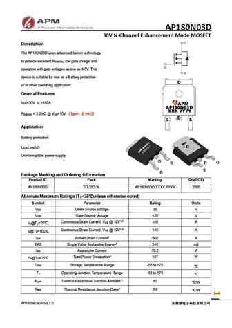
AP180N03D 30V N-Channel Enhancement Mode MOSFET Description The AP180N03D uses advanced trench technology to provide excellent R , low gate charge and DS(ON) operation with gate voltages as low as 4.5V. This device is suitable for use as a Battery protection or in other Switching application. General Features V =30V I =180A DS D R
ap180n03p ap180n03t.pdf
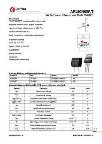
AP180N03PIT 30V N-Channel Enhancement Mode MOSFET Description The AP180N03P/T uses advanced trench technology to provide excellent R , low gate charge and DS(ON) operation with gate voltages as low as 4.5V. This device is suitable for use as a Battery protection or in other Switching application. General Features V = 30V I =180 A DS D R
ap80n03df.pdf
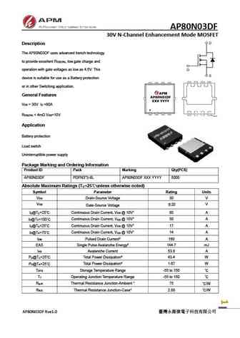
AP80N03DF 30V N-Channel Enhancement Mode MOSFET Description The AP80N03DF uses advanced trench technology to provide excellent R , low gate charge and DS(ON) operation with gate voltages as low as 4.5V. This device is suitable for use as a Battery protection or in other Switching application. General Features V = 30V I =80A DS D R
ap80n03d.pdf
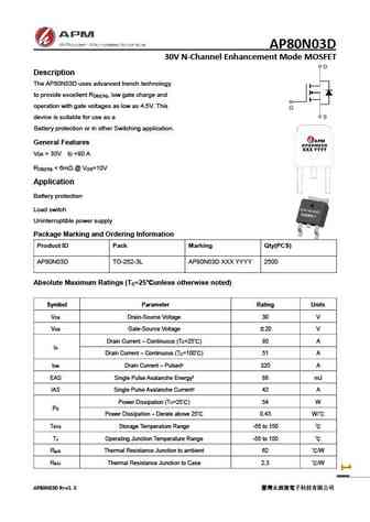
AP80N03D 30V N-Channel Enhancement Mode MOSFET Description The AP80N03D uses advanced trench technology to provide excellent R , low gate charge and DS(ON) operation with gate voltages as low as 4.5V. This device is suitable for use as a Battery protection or in other Switching application. General Features V = 30V I =80 A DS D R
ap80n03nf.pdf
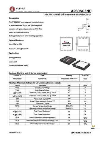
AP80N03NF 30V N-Channel Enhancement Mode MOSFET Description The AP80N03NF uses advanced trench technology to provide excellent R , low gate charge and DS(ON) operation with gate voltages as low as 4.5V. This device is suitable for use as a Battery protection or in other Switching application. General Features V = 30V I =80A DS D R
Otros transistores... 40N10K , 40P04 , 45P40 , 50N03 , 5P40 , 60N04 , 6706A , 68P40 , EMB04N03H , 80N04 , 80N08TR , 8205A , 8205B , G3205 , G1010 , G3710 , 5N20A .
History: IXFA20N85XHV
History: IXFA20N85XHV
🌐 : EN ES РУ
Liste
Recientemente añadidas las descripciónes de los transistores:
MOSFET: ASU70R600E | ASU65R850E | ASU65R550E | ASU65R350E | ASR65R120EFD | ASR65R046EFD | ASQ65R046EFD | ASM65R280E | ASM60R330E | ASE70R950E | ASD80R750E | ASD70R950E | ASD70R600E | ASD70R380E | ASD65R850E | ASD65R550E
Popular searches
60r190p datasheet | cs30n20 datasheet | go42n10 | 2sa970 datasheet | 2sc1627 | aoe6936 datasheet | g40t60an3h datasheet | j5027-r datasheet
