FTK2333 MOSFET Equivalente. Reemplazo. Hoja de especificaciones. Principales características
Número de Parte: FTK2333
Tipo de FET: MOSFET
Polaridad de transistor: P
ESPECIFICACIONES MÁXIMAS
Pdⓘ - Máxima disipación de potencia: 0.35 W
|Vds|ⓘ - Voltaje máximo drenador-fuente: 12 V
|Vgs|ⓘ - Voltaje máximo fuente-puerta: 8 V
|Id|ⓘ - Corriente continua de drenaje: 6 A
Tjⓘ - Temperatura máxima de unión: 150 °C
CARACTERÍSTICAS ELÉCTRICAS
trⓘ - Tiempo de subida: 24 nS
Cossⓘ - Capacitancia de salida: 255 pF
RDSonⓘ - Resistencia estado encendido drenaje a fuente: 0.028 Ohm
Encapsulados: SOT23
Búsqueda de reemplazo de FTK2333 MOSFET
- Selecciónⓘ de transistores por parámetros
FTK2333 datasheet
ftk2333.pdf
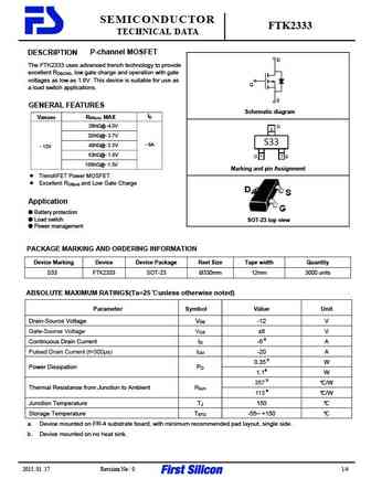
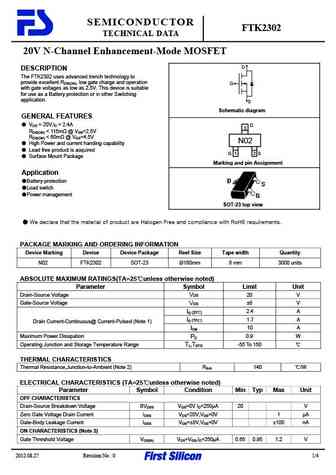
SEMICONDUCTOR FTK2333 TECHNICAL DATA P-channel MOSFET DESCRIPTION D The FTK2333 uses advanced trench technology to provide excellent RDS(ON), low gate charge and operation with gate voltages as low as 1.8V. This device is suitable for use as G a load switch applications. S GENERAL FEATURES Schematic diagram ID V(BR)DSS RDS(on) MAX 28m @ -4.5V 32m @-3.7V S33 -6A 4
ftk2341e.pdf
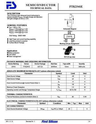
SEMICONDUCTOR FTK2341E TECHNICAL DATA DESCRIPTION The FTK2341E uses advanced trench technology to provide excellent RDS(ON), low gate charge and operation with gate voltages as low as -2.5V. GENERAL FEATURES VDS = -20V,ID =-4A Schematic diagram RDS(ON)
ftk2306a.pdf
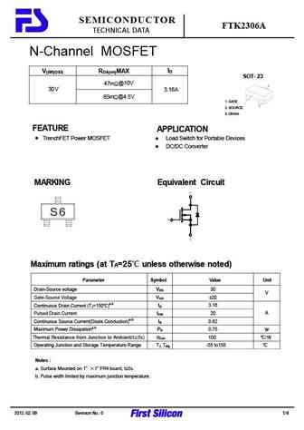
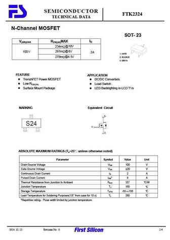
SEMICONDUCTOR FTK2306A TECHNICAL DATA N-Channel MOSFET ID V(BR)DSS RDS(on)MAX SOT-23 47m @10V 30V 3.16A 65m @4.5V 1. GATE 2. SOURCE 3. DRAIN FEATURE APPLICATION TrenchFET Power MOSFET Load Switch for Portable Devices DC/DC Converter MARKING Equivalent Circuit Maximum ratings (at TA=25 unless otherwise noted) Parameter Symbol Value Unit Drain-Source
ftk2304.pdf
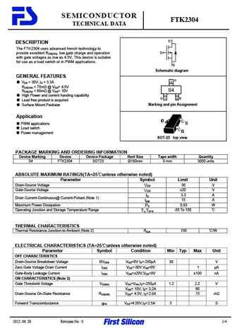
SEMICONDUCTOR FTK2304 TECHNICAL DATA D DESCRIPTION The FTK2304 uses advanced trench technology to G provide excellent RDS(ON), low gate charge and operation with gate voltages as low as 4.5V. This device is suitable for use as a load switch or in PWM applications. S Schematic diagram GENERAL FEATURES D VDS = 30V ,ID = 3.3A 3 RDS(ON)
Otros transistores... FTK2301, FTK2302, FTK2304, FTK2306, FTK2306A, FTK2310, FTK2312, FTK2324, K2611, FTK2341E, FTK25N03PDFN33, FTK2627, FTK2816E, FTK3004D, FTK3018, FTK3022, FTK3051
🌐 : EN ES РУ

Liste
Recientemente añadidas las descripciónes de los transistores:
MOSFET: SVF11N65F | SVF11N65T | FKBB3105 | EHBA036R1 | CRTT067N10N | AP6NA3R2MT | AP65SA145DDT8 | AP4NAR95CMT-A | AP4024GEMT-HF | AP3P050AH | AP3P020H | AP3N9R5YT | AP3N9R5MT | AP3N5R0MT | AP2P053Y | AP12A390YT
Popular searches
2sd313 | 2sc536 | d718 transistor | irfp250n datasheet | 2n5550 | 2sd1047 | 2n3035 | ksc1815