FTK2333 Specs and Replacement
Type Designator: FTK2333
Type of Transistor: MOSFET
Type of Control Channel: P-Channel
Absolute Maximum Ratings
Pd ⓘ - Maximum Power Dissipation: 0.35 W
|Vds|ⓘ - Maximum Drain-Source Voltage: 12 V
|Vgs|ⓘ - Maximum Gate-Source Voltage: 8 V
|Id| ⓘ - Maximum Drain Current: 6 A
Tj ⓘ - Maximum Junction Temperature: 150 °C
Electrical Characteristics
tr ⓘ - Rise Time: 24 nS
Cossⓘ - Output Capacitance: 255 pF
RDSonⓘ - Maximum Drain-Source On-State Resistance: 0.028 Ohm
Package: SOT23
FTK2333 substitution
- MOSFET ⓘ Cross-Reference Search
FTK2333 datasheet
ftk2333.pdf
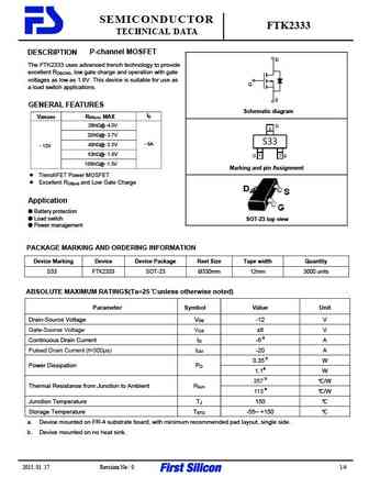
SEMICONDUCTOR FTK2333 TECHNICAL DATA P-channel MOSFET DESCRIPTION D The FTK2333 uses advanced trench technology to provide excellent RDS(ON), low gate charge and operation with gate voltages as low as 1.8V. This device is suitable for use as G a load switch applications. S GENERAL FEATURES Schematic diagram ID V(BR)DSS RDS(on) MAX 28m @ -4.5V 32m @-3.7V S33 -6A 4... See More ⇒
ftk2341e.pdf
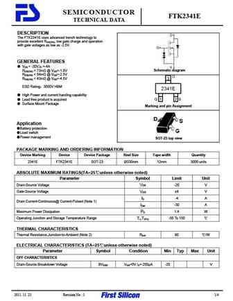
SEMICONDUCTOR FTK2341E TECHNICAL DATA DESCRIPTION The FTK2341E uses advanced trench technology to provide excellent RDS(ON), low gate charge and operation with gate voltages as low as -2.5V. GENERAL FEATURES VDS = -20V,ID =-4A Schematic diagram RDS(ON) ... See More ⇒
ftk2306a.pdf
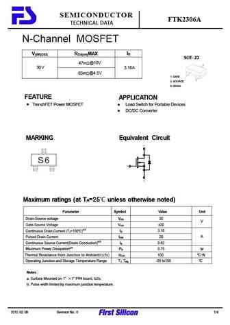
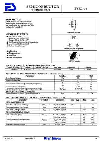
SEMICONDUCTOR FTK2306A TECHNICAL DATA N-Channel MOSFET ID V(BR)DSS RDS(on)MAX SOT-23 47m @10V 30V 3.16A 65m @4.5V 1. GATE 2. SOURCE 3. DRAIN FEATURE APPLICATION TrenchFET Power MOSFET Load Switch for Portable Devices DC/DC Converter MARKING Equivalent Circuit Maximum ratings (at TA=25 unless otherwise noted) Parameter Symbol Value Unit Drain-Source... See More ⇒
ftk2304.pdf
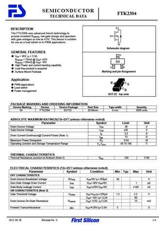
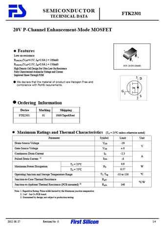
SEMICONDUCTOR FTK2304 TECHNICAL DATA D DESCRIPTION The FTK2304 uses advanced trench technology to G provide excellent RDS(ON), low gate charge and operation with gate voltages as low as 4.5V. This device is suitable for use as a load switch or in PWM applications. S Schematic diagram GENERAL FEATURES D VDS = 30V ,ID = 3.3A 3 RDS(ON) ... See More ⇒
Detailed specifications: FTK2301, FTK2302, FTK2304, FTK2306, FTK2306A, FTK2310, FTK2312, FTK2324, K2611, FTK2341E, FTK25N03PDFN33, FTK2627, FTK2816E, FTK3004D, FTK3018, FTK3022, FTK3051
Keywords - FTK2333 MOSFET specs
FTK2333 cross reference
FTK2333 equivalent finder
FTK2333 pdf lookup
FTK2333 substitution
FTK2333 replacement
Can't find your MOSFET? Learn how to find a substitute transistor by analyzing voltage, current and package compatibility
🌐 : EN ES РУ

LIST
Last Update
MOSFET: SVF11N65F | SVF11N65T | FKBB3105 | EHBA036R1 | CRTT067N10N | AP6NA3R2MT | AP65SA145DDT8 | AP4NAR95CMT-A | AP4024GEMT-HF | AP3P050AH
Popular searches
2sd313 | 2sc536 | d718 transistor | irfp250n datasheet | 2n5550 | 2sd1047 | 2n3035 | ksc1815