FTK3443 MOSFET Equivalente. Reemplazo. Hoja de especificaciones. Principales características
Número de Parte: FTK3443
Tipo de FET: MOSFET
Polaridad de transistor: P
ESPECIFICACIONES MÁXIMAS
Pdⓘ - Máxima disipación de potencia: 0.35 W
|Vds|ⓘ - Voltaje máximo drenador-fuente: 20 V
|Vgs|ⓘ - Voltaje máximo fuente-puerta: 8 V
|Id|ⓘ - Corriente continua de drenaje: 4 A
Tjⓘ - Temperatura máxima de unión: 150 °C
CARACTERÍSTICAS ELÉCTRICAS
trⓘ - Tiempo de subida: 30 nS
Cossⓘ - Capacitancia de salida: 180 pF
RDSonⓘ - Resistencia estado encendido drenaje a fuente: 0.065 Ohm
Encapsulados: SOT23-6
Búsqueda de reemplazo de FTK3443 MOSFET
- Selecciónⓘ de transistores por parámetros
FTK3443 datasheet
ftk3443.pdf
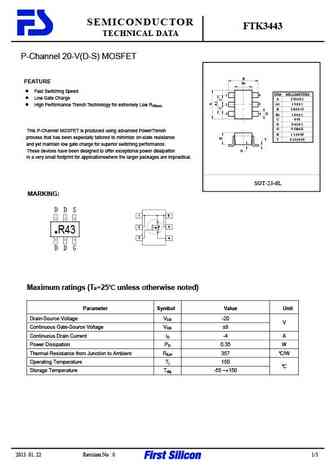
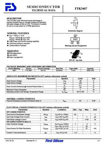
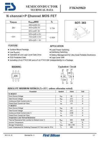
SEMICONDUCTOR FTK3443 TECHNICAL DATA P-Channel 20-V(D-S) MOSFET B FEATURE B1 Fast Switching Speed DIM MILLIMETERS 1 6 Low Gate Charge A 2 92 0 1 2 5 A1 1 9 0 1 High Performance Trench Technology for extremely Low RDS(on) B 2 8 0 15 3 4 D B1 1 6 0 1 C 0 95 D 0 4 0 1 G 0 1MAX This P-Channel MOSFET is produced using advanced PowerTrench H 1 1 0 05 process tha
ftk3415l.pdf
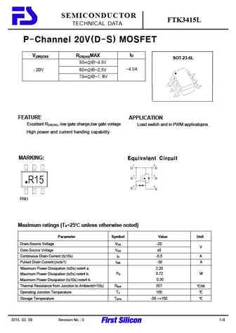
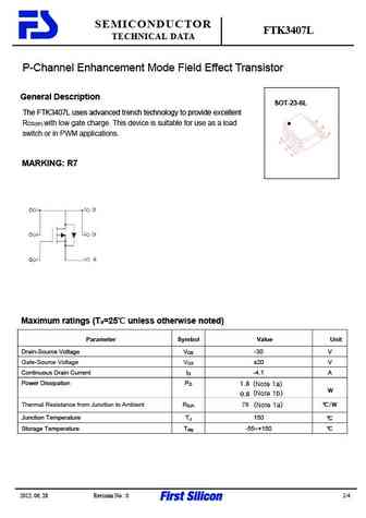
SEMICONDUCTOR FTK3415L TECHNICAL DATA P-Channel 20V(D-S) MOSFET ID V(BR)DSS RDS(on)MAX SOT-23-6L 50m @-4.5V -4.0A -20V 60m @-2.5V 73m @-1. 8V FEATURE APPLICATION Excellent RDS(ON), low gate charge,low gate voltage Load switch and in PWM applicatopns High power and current handing capability MARKING Equivalent Circuit PIN1 Maximum ratings (Ta=25 unless otherwise
ftk3400.pdf
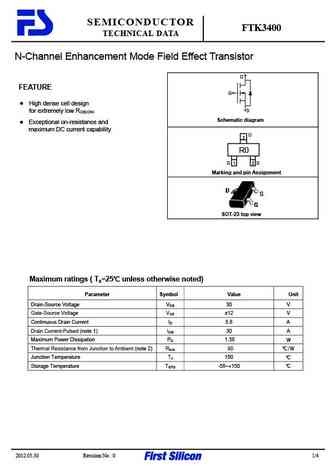
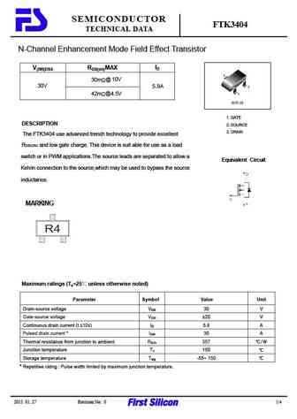
SEMICONDUCTOR FTK3400 TECHNICAL DATA N-Channel Enhancement Mode Field Effect Transistor D FEATURE G High dense cell design for extremely low R S DS(ON) Schematic diagram Exceptional on-resistance and maximum DC current capability D 3 R0 G 1 2 S Marking and pin Assignment SOT-23 top view Maximum ratings ( Ta=25 unless otherwise noted) Parameter Symbol Value Unit
ftk3415.pdf
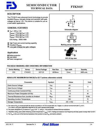
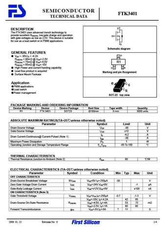
SEMICONDUCTOR FTK3415 TECHNICAL DATA DESCRIPTION D The FTK3415 uses advanced trench technology to provide excellent RDS(ON), low gate charge and operation with gate voltages as low as 1.8V. This device is suitable for use as G a load switch applications. S GENERAL FEATURES Schematic diagram VDS = -20V,ID =-4A RDS(ON)
Otros transistores... FTK3400, FTK3401, FTK3404, FTK3407, FTK3407L, FTK3415, FTK3415L, FTK3439KD, IRF1404, FTK35N03PDFN33, FTK35N03PDFN56, FTK3610, FTK3615, FTK3620, FTK3N80I, FTK3N80D, FTK3N80P
🌐 : EN ES РУ

Liste
Recientemente añadidas las descripciónes de los transistores:
MOSFET: AUW033N08BG | AUW025N10 | AUR030N10 | AUR020N10 | AUR020N085 | AUR014N10 | AUP074N10 | AUP065N10 | AUP062N08BG | AUP060N08AG | HYG053N10NS1B | HYG053N10NS1P | AP220N04T | AP220N04P | QM3126M3 | AUP060N055
Popular searches
tip3055 transistor | irf530 datasheet | 2sc2625 | 2sc1815 transistor | 2sd718 | 2n3053 transistor | 2sc458 replacement | bc557 transistor