FTK3443 Specs and Replacement
Type Designator: FTK3443
Type of Transistor: MOSFET
Type of Control Channel: P-Channel
Absolute Maximum Ratings
Pd ⓘ - Maximum Power Dissipation: 0.35 W
|Vds|ⓘ - Maximum Drain-Source Voltage: 20 V
|Vgs|ⓘ - Maximum Gate-Source Voltage: 8 V
|Id| ⓘ - Maximum Drain Current: 4 A
Tj ⓘ - Maximum Junction Temperature: 150 °C
Electrical Characteristics
tr ⓘ - Rise Time: 30 nS
Cossⓘ - Output Capacitance: 180 pF
RDSonⓘ - Maximum Drain-Source On-State Resistance: 0.065 Ohm
Package: SOT23-6
FTK3443 substitution
- MOSFET ⓘ Cross-Reference Search
FTK3443 datasheet
ftk3443.pdf
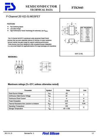
SEMICONDUCTOR FTK3443 TECHNICAL DATA P-Channel 20-V(D-S) MOSFET B FEATURE B1 Fast Switching Speed DIM MILLIMETERS 1 6 Low Gate Charge A 2 92 0 1 2 5 A1 1 9 0 1 High Performance Trench Technology for extremely Low RDS(on) B 2 8 0 15 3 4 D B1 1 6 0 1 C 0 95 D 0 4 0 1 G 0 1MAX This P-Channel MOSFET is produced using advanced PowerTrench H 1 1 0 05 process tha... See More ⇒
ftk3415l.pdf
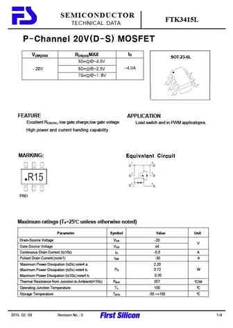
SEMICONDUCTOR FTK3415L TECHNICAL DATA P-Channel 20V(D-S) MOSFET ID V(BR)DSS RDS(on)MAX SOT-23-6L 50m @-4.5V -4.0A -20V 60m @-2.5V 73m @-1. 8V FEATURE APPLICATION Excellent RDS(ON), low gate charge,low gate voltage Load switch and in PWM applicatopns High power and current handing capability MARKING Equivalent Circuit PIN1 Maximum ratings (Ta=25 unless otherwise ... See More ⇒
ftk3400.pdf
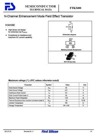
SEMICONDUCTOR FTK3400 TECHNICAL DATA N-Channel Enhancement Mode Field Effect Transistor D FEATURE G High dense cell design for extremely low R S DS(ON) Schematic diagram Exceptional on-resistance and maximum DC current capability D 3 R0 G 1 2 S Marking and pin Assignment SOT-23 top view Maximum ratings ( Ta=25 unless otherwise noted) Parameter Symbol Value Unit ... See More ⇒
ftk3415.pdf
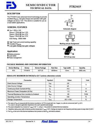
SEMICONDUCTOR FTK3415 TECHNICAL DATA DESCRIPTION D The FTK3415 uses advanced trench technology to provide excellent RDS(ON), low gate charge and operation with gate voltages as low as 1.8V. This device is suitable for use as G a load switch applications. S GENERAL FEATURES Schematic diagram VDS = -20V,ID =-4A RDS(ON) ... See More ⇒
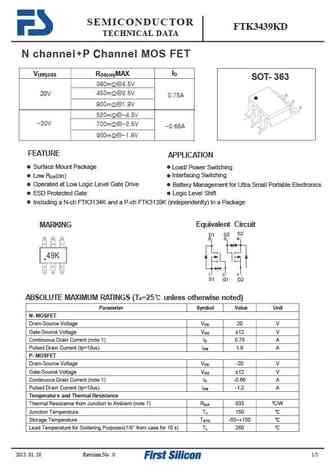
Detailed specifications: FTK3400, FTK3401, FTK3404, FTK3407, FTK3407L, FTK3415, FTK3415L, FTK3439KD, IRF1404, FTK35N03PDFN33, FTK35N03PDFN56, FTK3610, FTK3615, FTK3620, FTK3N80I, FTK3N80D, FTK3N80P
Keywords - FTK3443 MOSFET specs
FTK3443 cross reference
FTK3443 equivalent finder
FTK3443 pdf lookup
FTK3443 substitution
FTK3443 replacement
Step-by-step guide to finding a MOSFET replacement. Cross-reference parts and ensure compatibility for your repair or project.
🌐 : EN ES РУ

LIST
Last Update
MOSFET: AUW033N08BG | AUW025N10 | AUR030N10 | AUR020N10 | AUR020N085 | AUR014N10 | AUP074N10 | AUP065N10 | AUP062N08BG | AUP060N08AG
Popular searches
tip3055 transistor | irf530 datasheet | 2sc2625 | 2sc1815 transistor | 2sd718 | 2n3053 transistor | 2sc458 replacement | bc557 transistor