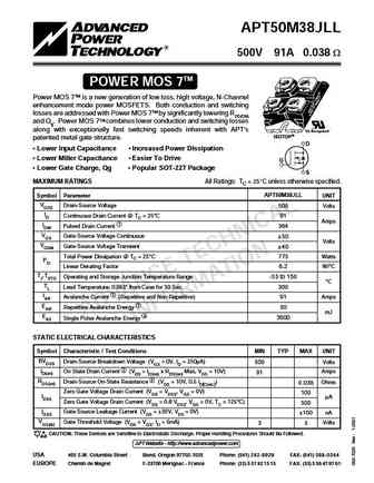
APT50M38JLL MOSFET Equivalente. Reemplazo. Hoja de especificaciones. Principales características
Número de Parte: APT50M38JLL
Tipo de FET: MOSFET
Polaridad de transistor: N
ESPECIFICACIONES MÁXIMAS
Pdⓘ - Máxima disipación de potencia: 775 W
|Vds|ⓘ - Voltaje máximo drenador-fuente: 500 V
|Vgs|ⓘ - Voltaje máximo fuente-puerta: 30 V
|Id|ⓘ - Corriente continua de drenaje: 91 A
Tjⓘ - Temperatura máxima de unión: 150 °C
CARACTERÍSTICAS ELÉCTRICAS
trⓘ - Tiempo de subida: 18 nS
Cossⓘ - Capacitancia de salida: 2610 pF
RDSonⓘ - Resistencia estado encendido drenaje a fuente: 0.038 Ohm
Encapsulados: SOT227
Búsqueda de reemplazo de APT50M38JLL MOSFET
- Selecciónⓘ de transistores por parámetros
APT50M38JLL datasheet
apt50m38jll.pdf
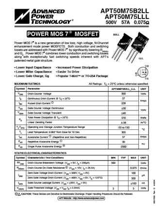
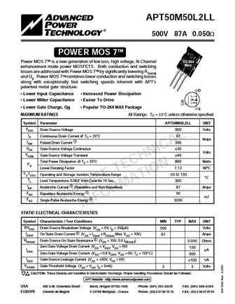
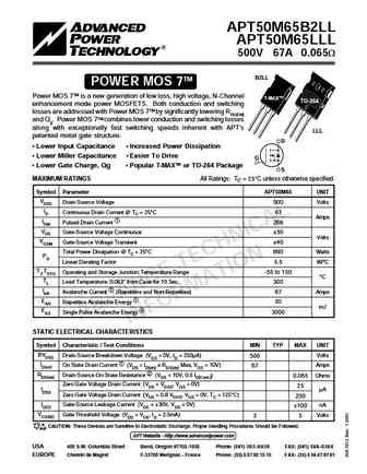
APT50M38JLL 500V 91A 0.038 W TM POWER MOS 7 Power MOS 7TM is a new generation of low loss, high voltage, N-Channel enhancement mode power MOSFETS. Both conduction and switching losses are addressed with Power MOS 7TM by significantly lowering RDS(ON) and Qg. Power MOS 7TM combines lower conduction and switching losses along with exceptionally fast switching speeds inherent with APT's
apt50m38jfll.pdf
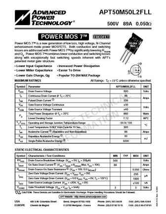
APT50M38JFLL 500V 91A 0.038W TM FREDFET POWER MOS 7 Power MOS 7TM is a new generation of low loss, high voltage, N-Channel enhancement mode power MOSFETS. Both conduction and switching losses are addressed with Power MOS 7TM by significantly lowering RDS(ON) and Qg. Power MOS 7TM combines lower conduction and switching losses along with exceptionally fast switching speeds inherent wit
apt50m80.pdf
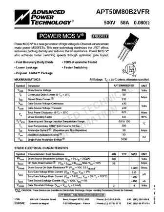
APT50M80B2VFR 500V 58A 0.080W POWER MOS V FREDFET T-MAX Power MOS V is a new generation of high voltage N-Channel enhancement mode power MOSFETs. This new technology minimizes the JFET effect, increases packing density and reduces the on-resistance. Power MOS V also achieves faster switching speeds through optimized gate layout. Fast Recovery Body Diode 100% Avalanche T
apt50m50jll.pdf
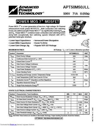
APT50M50JLL 500V 71A 0.050 R POWER MOS 7 MOSFET Power MOS 7 is a new generation of low loss, high voltage, N-Channel enhancement mode power MOSFETS. Both conduction and switching losses are addressed with Power MOS 7 by significantly lowering RDS(ON) and Qg. Power MOS 7 combines lower conduction and switching losses "UL Recognized" along with exceptionally
apt50m60jn.pdf
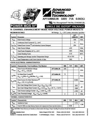
D G APT50M60JN 500V 71A 0.06O S "UL Recognized" File No. E145592 (S) ISOTOP POWER MOS IV SINGLE DIE ISOTOP PACKAGE N- CHANNEL ENHANCEMENT MODE HIGH VOLTAGE POWER MOSFETS MAXIMUM RATINGS All Ratings TC = 25 C unless otherwise specified. APT Symbol Parameter 50M60JN UNIT VDSS Drain-Source Voltage 500 Volts ID Continuous Drain Current @ TC = 25 C 71 Amps IDM, lLM Pulse
apt50m80b2vfr.pdf
APT50M80B2VFR 500V 58A 0.080W POWER MOS V FREDFET T-MAX Power MOS V is a new generation of high voltage N-Channel enhancement mode power MOSFETs. This new technology minimizes the JFET effect, increases packing density and reduces the on-resistance. Power MOS V also achieves faster switching speeds through optimized gate layout. Fast Recovery Body Diode 100% Avalanche T
apt50m65jll.pdf
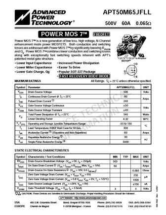
APT50M65JLL 500V 60A 0.065 W TM POWER MOS 7 Power MOS 7TM is a new generation of low loss, high voltage, N-Channel enhancement mode power MOSFETS. Both conduction and switching losses are addressed with Power MOS 7TM by significantly lowering RDS(ON) and Qg. Power MOS 7TM combines lower conduction and switching losses along with exceptionally fast switching speeds inherent with APT's
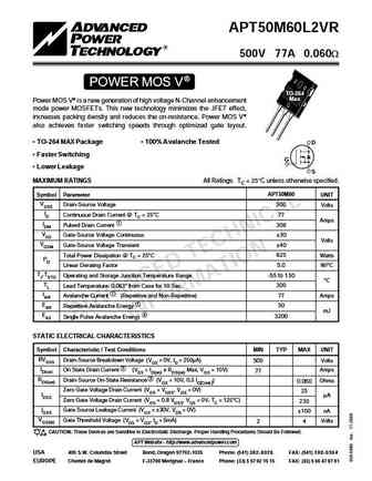
apt50m60l2vfr.pdf
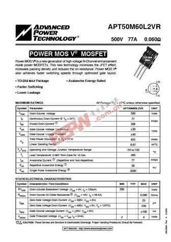
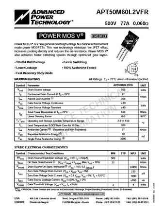
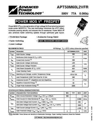
APT50M60L2VFR 500V 77A 0.060W POWER MOS V FREDFET TO-264 Max Power MOS V is a new generation of high voltage N-Channel enhancement mode power MOSFETs. This new technology minimizes the JFET effect, increases packing density and reduces the on-resistance. Power MOS V also achieves faster switching speeds through optimized gate layout. TO-264 MAX Package Faster Switching D
apt50m50pvr.pdf
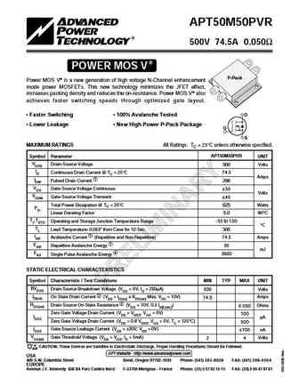
APT50M50PVR 500V 74.5A 0.050 POWER MOS V P-Pack Power MOS V is a new generation of high voltage N-Channel enhancement mode power MOSFETs. This new technology minimizes the JFET effect, increases packing density and reduces the on-resistance. Power MOS V also achieves faster switching speeds through optimized gate layout. Faster Switching 100% Avalanche Tested D Low
apt50m75b2ll.pdf
APT50M75B2LL APT50M75LLL 500V 57A 0.075W B2LL TM POWER MOS 7 Power MOS 7TM is a new generation of low loss, high voltage, N-Channel T-MAX TO-264 enhancement mode power MOSFETS. Both conduction and switching losses are addressed with Power MOS 7TM by significantly lowering RDS(ON) and Qg. Power MOS 7TM combines lower conduction and switching losses along with exceptionally fast s
apt50m80b2vfrg apt50m80lvfrg.pdf
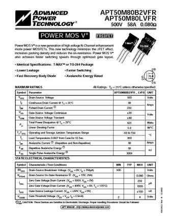
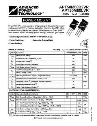
APT50M80B2VFR APT50M80LVFR 500V 58A 0.080 POWER MOS V FREDFET TM T-Max Power MOS V is a new generation of high voltage N-Channel enhancement TO-264 mode power MOSFETs. This new technology minimizes the JFET effect, increases packing density and reduces the on-resistance. Power MOS V also achieves faster switching speeds through optimized gate layout.
apt50m85jvr.pdf
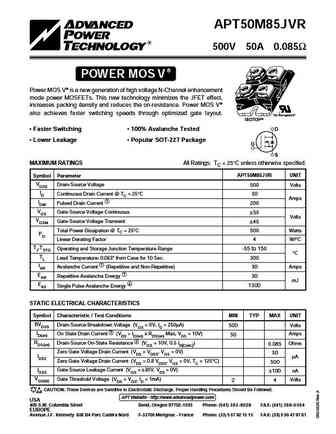
APT50M85JVR 500V 50A 0.085 POWER MOS V Power MOS V is a new generation of high voltage N-Channel enhancement mode power MOSFETs. This new technology minimizes the JFET effect, increases packing density and reduces the on-resistance. Power MOS V also achieves faster switching speeds through optimized gate layout. "UL Recognized" ISOTOP Faster Switching 100% Avalanche
apt50m80jlc.pdf
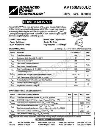
APT50M80JLC 500V 52A 0.080 W TM POWER MOS VI Power MOS VITM is a new generation of low gate charge, high voltage N-Channel enhancement mode power MOSFETs. Lower gate charge is achieved by optimizing the manufacturing process to minimize Ciss and Crss. Lower gate charge coupled with Power MOS VITM optimized gate layout, "UL Recognized" delivers exceptionally fast switching speeds. ISOT
apt50m75jfll.pdf
APT50M75JFLL 500V 52A 0.075W TM FREDFET POWER MOS 7 Power MOS 7TM is a new generation of low loss, high voltage, N-Channel enhancement mode power MOSFETS. Both conduction and switching losses are addressed with Power MOS 7TM by significantly lowering RDS(ON) and Qg. Power MOS 7TM combines lower conduction and switching losses along with exceptionally fast switching speeds inherent wit
apt50m50.pdf
APT50M50PVR 500V 74.5A 0.050 POWER MOS V P-Pack Power MOS V is a new generation of high voltage N-Channel enhancement mode power MOSFETs. This new technology minimizes the JFET effect, increases packing density and reduces the on-resistance. Power MOS V also achieves faster switching speeds through optimized gate layout. Faster Switching 100% Avalanche Tested D Low
apt50m60l2vfrg.pdf
APT50M60L2VFR 500V 77A 0.060 POWER MOS V FREDFET TO-264 Max Power MOS V is a new generation of high voltage N-Channel enhancement mode power MOSFETs. This new technology minimizes the JFET effect, increases packing density and reduces the on-resistance. Power MOS V also achieves faster switching speeds through optimized gate layout. D TO-264 MAX Packa
apt50m60jvfr.pdf
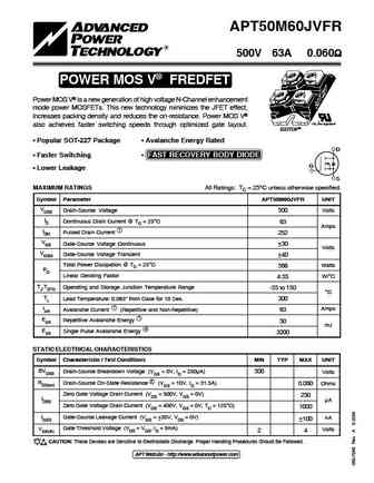
APT50M60JVFR 500V 63A 0.060 POWER MOS V FREDFET Power MOS V is a new generation of high voltage N-Channel enhancement mode power MOSFETs. This new technology minimizes the JFET effect, increases packing density and reduces the on-resistance. Power MOS V "UL Recognized" also achieves faster switching speeds through optimized gate layout. ISOTOP Popula
apt50m65lfll.pdf
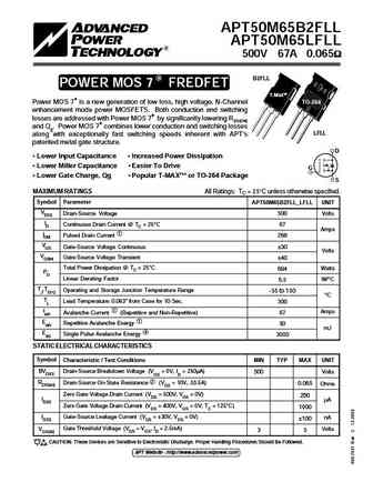
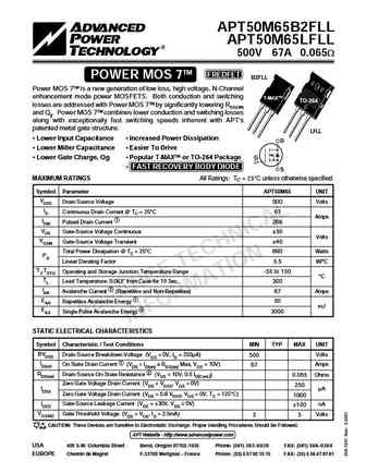
APT50M65B2FLL APT50M65LFLL 500V 67A 0.065 R B2FLL POWER MOS 7 FREDFET T-MaxTM Power MOS 7 is a new generation of low loss, high voltage, N-Channel TO-264 enhancement mode power MOSFETS. Both conduction and switching losses are addressed with Power MOS 7 by significantly lowering RDS(ON) and Qg. Power MOS 7 combines lower conduction and switching losses L
apt50m85b2vfr.pdf
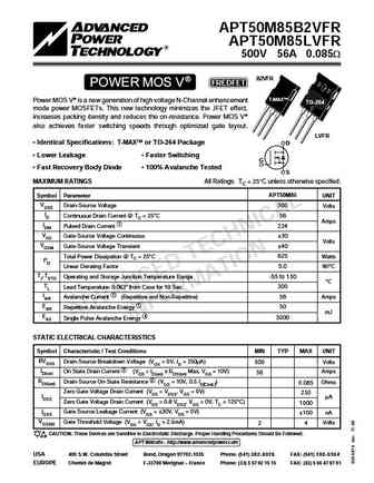
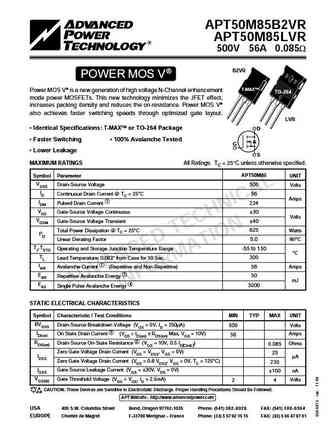
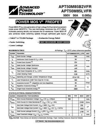
APT50M85B2VFR APT50M85LVFR 500V 56A 0.085W B2VFR POWER MOS V FREDFET T-MAX Power MOS V is a new generation of high voltage N-Channel enhancement TO-264 mode power MOSFETs. This new technology minimizes the JFET effect, increases packing density and reduces the on-resistance. Power MOS V also achieves faster switching speeds through optimized gate layout. LVFR Identical
apt50m75b2llg apt50m75lllg.pdf
APT50M75B2LL APT50M75LLL 500V 57A 0.075 R B2LL POWER MOS 7 MOSFET Power MOS 7 is a new generation of low loss, high voltage, N-Channel T-MAX TO-264 enhancement mode power MOSFETS. Both conduction and switching losses are addressed with Power MOS 7 by significantly lowering RDS(ON) and Qg. Power MOS 7 combines lower conduction and switching losses alo
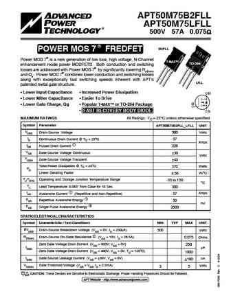
apt50m75b2fllg apt50m75lfllg.pdf
APT50M75B2FLL APT50M75LFLL 500V 57A 0.075 R B2FLL POWER MOS 7 FREDFET Power MOS 7 is a new generation of low loss, high voltage, N-Channel T-MAX TO-264 enhancement mode power MOSFETS. Both conduction and switching losses are addressed with Power MOS 7 by significantly lowering RDS(ON) and Qg. Power MOS 7 combines lower conduction and switching losses
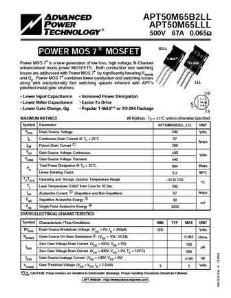
apt50m65b2llg apt50m65lllg.pdf
APT50M65B2LL APT50M65LLL 500V 67A 0.065 R B2LL POWER MOS 7 MOSFET T-MaxTM Power MOS 7 is a new generation of low loss, high voltage, N-Channel TO-264 enhancement mode power MOSFETS. Both conduction and switching losses are addressed with Power MOS 7 by significantly lowering RDS(ON) and Qg. Power MOS 7 combines lower conduction and switching losses LLL
apt50m65.pdf
APT50M65B2FLL APT50M65LFLL 500V 67A 0.065W TM FREDFET POWER MOS 7 B2FLL Power MOS 7TM is a new generation of low loss, high voltage, N-Channel enhancement mode power MOSFETS. Both conduction and switching T-MAX TO-264 losses are addressed with Power MOS 7TM by significantly lowering RDS(ON) and Qg. Power MOS 7TM combines lower conduction and switching losses along with exceptio
apt50m50l2llg.pdf
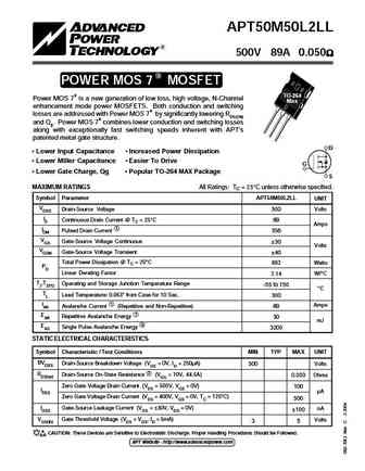
APT50M50L2LL 500V 89A 0.050 R POWER MOS 7 MOSFET TO-264 Power MOS 7 is a new generation of low loss, high voltage, N-Channel Max enhancement mode power MOSFETS. Both conduction and switching losses are addressed with Power MOS 7 by significantly lowering RDS(ON) and Qg. Power MOS 7 combines lower conduction and switching losses along with exceptionally fa
apt50m75jll.pdf
APT50M75JLL 500V 52A 0.075 W TM POWER MOS 7 Power MOS 7TM is a new generation of low loss, high voltage, N-Channel enhancement mode power MOSFETS. Both conduction and switching losses are addressed with Power MOS 7TM by significantly lowering RDS(ON) and Qg. Power MOS 7TM combines lower conduction and switching losses along with exceptionally fast switching speeds inherent with APT's
apt50m85lvr.pdf
APT50M85B2VR APT50M85LVR 500V 56A 0.085W B2VR POWER MOS V T-MAX Power MOS V is a new generation of high voltage N-Channel enhancement TO-264 mode power MOSFETs. This new technology minimizes the JFET effect, increases packing density and reduces the on-resistance. Power MOS V also achieves faster switching speeds through optimized gate layout. LVR Identical Specificatio
apt50m80b2vr.pdf
APT50M80B2VR APT50M80LVR 500V 58A 0.080W B2VR POWER MOS V T-MAX Power MOS V is a new generation of high voltage N-Channel enhancement TO-264 mode power MOSFETs. This new technology minimizes the JFET effect, increases packing density and reduces the on-resistance. Power MOS V also achieves faster switching speeds through optimized gate layout. LVR Identical Specificatio
apt50m60jvr.pdf
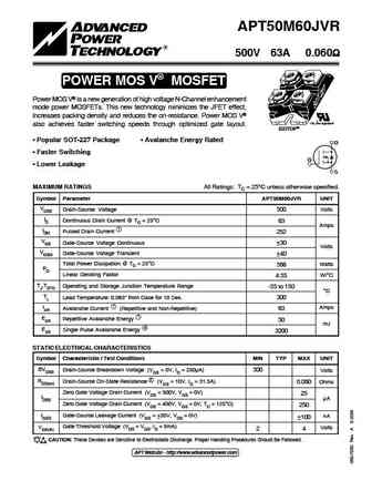
APT50M60JVR 500V 63A 0.060 POWER MOS V MOSFET Power MOS V is a new generation of high voltage N-Channel enhancement mode power MOSFETs. This new technology minimizes the JFET effect, increases packing density and reduces the on-resistance. Power MOS V "UL Recognized" also achieves faster switching speeds through optimized gate layout. ISOTOP Popular
apt50m85b2vr.pdf
APT50M85B2VR APT50M85LVR 500V 56A 0.085W B2VR POWER MOS V T-MAX Power MOS V is a new generation of high voltage N-Channel enhancement TO-264 mode power MOSFETs. This new technology minimizes the JFET effect, increases packing density and reduces the on-resistance. Power MOS V also achieves faster switching speeds through optimized gate layout. LVR Identical Specificatio
apt50m80b2lc.pdf
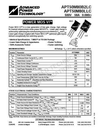
APT50M80B2LC APT50M80LLC 500V 58A 0.080W B2LC TM POWER MOS VI T-MAX Power MOS VITM is a new generation of low gate charge, high voltage TO-264 N-Channel enhancement mode power MOSFETs. Lower gate charge is achieved by optimizing the manufacturing process to minimize Ciss and Crss. Lower gate charge coupled with Power MOS VITM optimized gate layout, LLC delivers exceptionally fas
apt50m85b2vfrg apt50m85lvfrg.pdf
APT50M85B2VFR APT50M85LVFR 500V 56A 0.085 B2VFR POWER MOS V FREDFET T-MAX TO-264 Power MOS V is a new generation of high voltage N-Channel enhancement mode power MOSFETs. This new technology minimizes the JFET effect, increases packing density and reduces the on-resistance. Power MOS V also achieves faster switching speeds through optimized gate layout
apt50m65b2fll.pdf
APT50M65B2FLL APT50M65LFLL 500V 67A 0.065W TM FREDFET POWER MOS 7 B2FLL Power MOS 7TM is a new generation of low loss, high voltage, N-Channel enhancement mode power MOSFETS. Both conduction and switching T-MAX TO-264 losses are addressed with Power MOS 7TM by significantly lowering RDS(ON) and Qg. Power MOS 7TM combines lower conduction and switching losses along with exceptio
apt50m50jfll.pdf
APT50M50JFLL 500V 71A 0.050W TM FREDFET POWER MOS 7 Power MOS 7TM is a new generation of low loss, high voltage, N-Channel enhancement mode power MOSFETS. Both conduction and switching losses are addressed with Power MOS 7TM by significantly lowering RDS(ON) and Qg. Power MOS 7TM combines lower conduction and switching losses along with exceptionally fast switching speeds inherent wit
apt50m50l2fllg.pdf
APT50M50L2FLL 500V 89A 0.050 R POWER MOS 7 FREDFET TO-264 Power MOS 7 is a new generation of low loss, high voltage, N-Channel Max enhancement mode power MOSFETS. Both conduction and switching losses are addressed with Power MOS 7 by significantly lowering RDS(ON) and Qg. Power MOS 7 combines lower conduction and switching losses along with exceptionally
apt50m50jvr.pdf
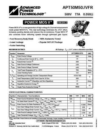
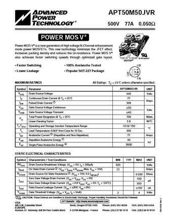
APT50M50JVR 500V 77A 0.050 POWER MOS V Power MOS V is a new generation of high voltage N-Channel enhancement mode power MOSFETs. This new technology minimizes the JFET effect, increases packing density and reduces the on-resistance. Power MOS V also achieves faster switching speeds through optimized gate layout. "UL Recognized" ISOTOP Faster Switching 100% Avalanche
apt50m50l2ll.pdf
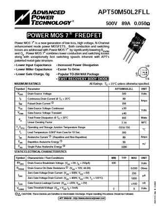
APT50M50L2LL 500V 87A 0.050W TM POWER MOS 7 Power MOS 7TM is a new generation of low loss, high voltage, N-Channel TO-264 Max enhancement mode power MOSFETS. Both conduction and switching losses are addressed with Power MOS 7TM by significantly lowering RDS(ON) and Qg. Power MOS 7TM combines lower conduction and switching losses along with exceptionally fast switching speeds inherent
apt50m50jlc.pdf
APT50M50JLC 500V 77A 0.050 W TM POWER MOS VI Power MOS VITM is a new generation of low gate charge, high voltage N-Channel enhancement mode power MOSFETs. Lower gate charge is achieved by optimizing the manufacturing process to minimize Ciss and Crss. Lower gate charge coupled with Power MOS VITM optimized gate layout, "UL Recognized" delivers exceptionally fast switching speeds. ISOT
apt50m50l2fll.pdf
APT50M50L2FLL 500V 89A 0.050W TM FREDFET POWER MOS 7 Power MOS 7TM is a new generation of low loss, high voltage, N-Channel TO-264 Max enhancement mode power MOSFETS. Both conduction and switching losses are addressed with Power MOS 7TM by significantly lowering RDS(ON) and Qg. Power MOS 7TM combines lower conduction and switching losses along with exceptionally fast switching speeds
apt50m65jfll.pdf
APT50M65JFLL 500V 60A 0.065W TM FREDFET POWER MOS 7 Power MOS 7TM is a new generation of low loss, high voltage, N-Channel enhancement mode power MOSFETS. Both conduction and switching losses are addressed with Power MOS 7TM by significantly lowering RDS(ON) and Qg. Power MOS 7TM combines lower conduction and switching losses along with exceptionally fast switching speeds inherent wit
apt50m75jllu2.pdf
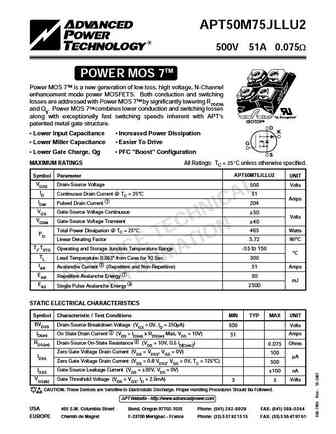
APT50M75JLLU2 APT50M75JLLU2 500V 51A 0.075W TM POWER MOS 7 Power MOS 7TM is a new generation of low loss, high voltage, N-Channel enhancement mode power MOSFETS. Both conduction and switching losses are addressed with Power MOS 7TM by significantly lowering RDS(ON) and Qg. Power MOS 7TM combines lower conduction and switching losses along with exceptionally fast switching speeds inher
apt50m65b2ll.pdf
APT50M65B2LL APT50M65LLL 500V 67A 0.065W B2LL TM POWER MOS 7 Power MOS 7TM is a new generation of low loss, high voltage, N-Channel T-MAX TO-264 enhancement mode power MOSFETS. Both conduction and switching losses are addressed with Power MOS 7TM by significantly lowering RDS(ON) and Qg. Power MOS 7TM combines lower conduction and switching losses along with exceptionally fast s
apt50m75b2fll.pdf
APT50M75B2FLL APT50M75LFLL 500V 57A 0.075W TM FREDFET POWER MOS 7 B2FLL Power MOS 7TM is a new generation of low loss, high voltage, N-Channel enhancement mode power MOSFETS. Both conduction and switching T-MAX TO-264 losses are addressed with Power MOS 7TM by significantly lowering RDS(ON) and Qg. Power MOS 7TM combines lower conduction and switching losses along with exceptio
apt50m80b2vrg apt50m80lvrg.pdf
APT50M80B2VR APT50M80LVR 500V 58A 0.080 POWER MOS V TM T-Max Power MOS V is a new generation of high voltage N-Channel enhancement TO-264 mode power MOSFETs. This new technology minimizes the JFET effect, increases packing density and reduces the on-resistance. Power MOS V also achieves faster switching speeds through optimized gate layout. Identical
apt50m75lfll.pdf
isc N-Channel MOSFET Transistor APT50M75LFLL FEATURES Drain Current I = 57A@ T =25 D C Drain Source Voltage- V =500V(Min) DSS Static Drain-Source On-Resistance R =0.075 (Max) DS(on) 100% avalanche tested Minimum Lot-to-Lot variations for robust device performance and reliable operation DESCRIPTION Designed for use in switch mode power supplies and general p
apt50m80b2vfr.pdf
isc N-Channel MOSFET Transistor APT50M80B2VFR FEATURES Drain Current I = 58A@ T =25 D C Drain Source Voltage- V =500V(Min) DSS Static Drain-Source On-Resistance R =0.08 (Max) DS(on) 100% avalanche tested Minimum Lot-to-Lot variations for robust device performance and reliable operation DESCRIPTION Designed for use in switch mode power supplies and general p
apt50m75b2ll.pdf
isc N-Channel MOSFET Transistor APT50M75B2LL FEATURES Drain Current I = 57A@ T =25 D C Drain Source Voltage- V =500V(Min) DSS Static Drain-Source On-Resistance R =0.075 (Max) DS(on) 100% avalanche tested Minimum Lot-to-Lot variations for robust device performance and reliable operation DESCRIPTION Designed for use in switch mode power supplies and general p
apt50m65lfll.pdf
isc N-Channel MOSFET Transistor APT50M65LFLL FEATURES Drain Current I = 67A@ T =25 D C Drain Source Voltage- V =500V(Min) DSS Static Drain-Source On-Resistance R =0.065 (Max) DS(on) 100% avalanche tested Minimum Lot-to-Lot variations for robust device performance and reliable operation DESCRIPTION Designed for use in switch mode power supplies and general p
apt50m80lvfr.pdf
isc N-Channel MOSFET Transistor APT50M80LVFR FEATURES Drain Current I = 58A@ T =25 D C Drain Source Voltage- V =500V(Min) DSS Static Drain-Source On-Resistance R =0.08 (Max) DS(on) 100% avalanche tested Minimum Lot-to-Lot variations for robust device performance and reliable operation DESCRIPTION Designed for use in switch mode power supplies and general pu
apt50m65b2fll.pdf
isc N-Channel MOSFET Transistor APT50M65B2FLL FEATURES Drain Current I = 67A@ T =25 D C Drain Source Voltage- V =500V(Min) DSS Static Drain-Source On-Resistance R =0.065 (Max) DS(on) 100% avalanche tested Minimum Lot-to-Lot variations for robust device performance and reliable operation DESCRIPTION Designed for use in switch mode power supplies and general
apt50m65b2ll.pdf
isc N-Channel MOSFET Transistor APT50M65B2LL FEATURES Drain Current I = 67A@ T =25 D C Drain Source Voltage- V =500V(Min) DSS Static Drain-Source On-Resistance R =0.065 (Max) DS(on) 100% avalanche tested Minimum Lot-to-Lot variations for robust device performance and reliable operation DESCRIPTION Designed for use in switch mode power supplies and general p
apt50m75b2fll.pdf
isc N-Channel MOSFET Transistor APT50M75B2FLL FEATURES Drain Current I = 57A@ T =25 D C Drain Source Voltage- V =500V(Min) DSS Static Drain-Source On-Resistance R =0.075 (Max) DS(on) 100% avalanche tested Minimum Lot-to-Lot variations for robust device performance and reliable operation DESCRIPTION Designed for use in switch mode power supplies and general
Otros transistores... IRFP151, IRFP152, IRFP153, IRFP22N50A, IRFP230, IRFP231, IRFP232, IRFP233, IRFZ44N, IRFP240, IRFP240A, IRFP240FI, IRFP241, IRFP242, IRFP243, IRFP244, IRFP244A
🌐 : EN ES РУ
Liste
Recientemente añadidas las descripciónes de los transistores:
MOSFET: AUW033N08BG | AUW025N10 | AUR030N10 | AUR020N10 | AUR020N085 | AUR014N10 | AUP074N10 | AUP065N10 | AUP062N08BG | AUP060N08AG | HYG053N10NS1B | HYG053N10NS1P | AP220N04T | AP220N04P | QM3126M3 | AUP060N055
Popular searches
lm317t datasheet | irf540 | bc337 | ksc1845 | c1815 transistor | 2sc1815 | irfz44 | 2n5551
