FDD6672A MOSFET Equivalente. Reemplazo. Hoja de especificaciones. Principales características
Número de Parte: FDD6672A
Tipo de FET: MOSFET
Polaridad de transistor: N
ESPECIFICACIONES MÁXIMAS
Pdⓘ - Máxima
disipación de potencia: 70 W
|Vds|ⓘ - Voltaje máximo drenador-fuente: 30 V
|Vgs|ⓘ - Voltaje máximo fuente-puerta: 12 V
|Id|ⓘ - Corriente continua
de drenaje: 65 A
Tjⓘ - Temperatura máxima de unión: 150 °C
CARACTERÍSTICAS ELÉCTRICAS
trⓘ - Tiempo
de subida: 18 nS
Cossⓘ - Capacitancia de salida: 550 pF
RDSonⓘ - Resistencia estado encendido drenaje a fuente: 0.008 Ohm
Encapsulados: TO-252
Búsqueda de reemplazo de FDD6672A MOSFET
- Selecciónⓘ de transistores por parámetros
FDD6672A datasheet
..1. Size:76K fairchild semi
fdd6672a.pdf 

April 2001 FDD6672A 30V N-Channel PowerTrench MOSFET General Description Features This N-Channel MOSFET has been designed 65 A, 30 V. RDS(ON) = 9.5 m @ VGS = 4.5 V specifically to improve the overall efficiency of DC/DC RDS(ON) = 8 m @ VGS = 10 V converters using either synchronous or conventional switching PWM controllers. It has been optimized for
..2. Size:287K inchange semiconductor
fdd6672a.pdf

isc N-Channel MOSFET Transistor FDD6672A FEATURES Drain Current I =65A@ T =25 D C Drain Source Voltage V =30V(Min) DSS Static Drain-Source On-Resistance R =8m (Max) @ V = 10V DS(on) GS 100% avalanche tested Minimum Lot-to-Lot variations for robust device performance and reliable operation DESCRIPTION motor drive, DC-DC converter, power switch and solenoid dr
8.1. Size:117K fairchild semi
fdd6676s.pdf
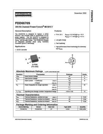
December 2002 FDD6676S 30V N-Channel PowerTrench MOSFET General Description Features The FDS6676S is designed to replace a DPAK 78 A, 30 V RDS(ON) = 6.0 m @ VGS = 10 V MOSFET and Schottky diode in synchronous DC DC RDS(ON) = 7.1 m @ VGS = 4.5 V power supplies. This 30V MOSFET is designed to maximize power conversion efficiency, providing a low Low gate charge
8.2. Size:91K fairchild semi
fdd6670s.pdf
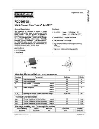
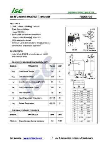
September 2001 FDD6670S 30V N-Channel PowerTrench SyncFET General Description Features The FDD6670S is designed to replace a single 64 A, 30 V RDS(ON) = 9 m @ VGS = 10 V MOSFET and Schottky diode in synchronous DC DC RDS(ON) = 12.5 m @ VGS = 4.5 V power supplies. This 30V MOSFET is designed to maximize power conversion efficiency, providing a low Includes S
8.3. Size:147K fairchild semi
fdd6670al.pdf

May 2004 FDD6670AL 30V N-Channel PowerTrench MOSFET General Description Features This N-Channel MOSFET has been designed 84 A, 30 V. RDS(ON) = 5 m @ VGS = 10 V specifically to improve the overall efficiency of DC/DC RDS(ON) = 6 m @ VGS = 4.5 V converters using either synchronous or conventional switching PWM controllers. It has been optimized for Low gate c
8.4. Size:80K fairchild semi
fdd6676.pdf
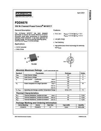
April 2001 FDD6676 30V N-Channel PowerTrench MOSFET General Description Features This N-Channel MOSFET has been designed 78 A, 30 V RDS(ON) = 7.5 m @ VGS = 10 V specifically to improve the overall efficiency of DC/DC RDS(ON) = 8.5 m @ VGS = 4.5 V converters using either synchronous or conventional switching PWM controllers. It has been optimized for
8.5. Size:105K fairchild semi
fdd6670as.pdf

May 2005 FDD6670AS 30V N-Channel PowerTrench SyncFET General Description Features The FDD6670AS is designed to replace a single 76 A, 30 V RDS(ON) max= 8.0 m @ VGS = 10 V MOSFET and Schottky diode in synchronous DC DC RDS(ON) max= 10.4 m @ VGS = 4.5 V power supplies. This 30V MOSFET is designed to maximize power conversion efficiency, providing a low Inclu
8.6. Size:109K fairchild semi
fdd6670a.pdf
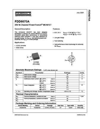
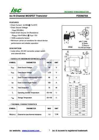
July 2005 FDD6670A 30V N-Channel PowerTrench MOSFET General Description Features This N-Channel MOSFET has been designed 66 A, 30 V RDS(ON) = 8 m @ VGS = 10 V specifically to improve the overall efficiency of DC/DC RDS(ON) = 10 m @ VGS = 4.5 V converters using either synchronous or conventional switching PWM controllers. It has been optimized for Low gate charge low ga
8.7. Size:411K fairchild semi
fdd6676as.pdf
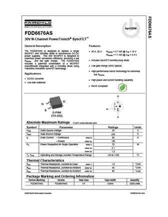
April 2008 FDD6676AS tm 30V N-Channel PowerTrench SyncFET General Description Features The FDD6676AS is designed to replace a single 90 A, 30 V RDS(ON) = 5.7 m @ VGS = 10 V MOSFET and Schottky diode in synchronous DC DC RDS(ON) = 7.1 m @ VGS = 4.5 V power supplies. This 30V MOSFET is designed to maximize power conversion efficiency, providing a low Includ
8.8. Size:287K inchange semiconductor
fdd6676s.pdf
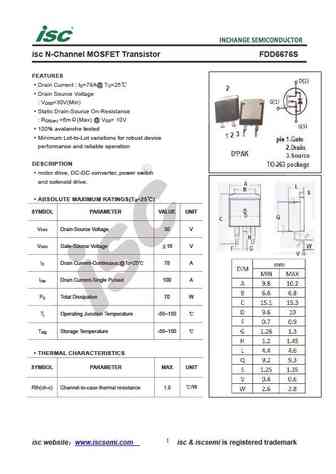
isc N-Channel MOSFET Transistor FDD6676S FEATURES Drain Current I =78A@ T =25 D C Drain Source Voltage V =30V(Min) DSS Static Drain-Source On-Resistance R =6m (Max) @ V = 10V DS(on) GS 100% avalanche tested Minimum Lot-to-Lot variations for robust device performance and reliable operation DESCRIPTION motor drive, DC-DC converter, power switch and solenoid dr
8.9. Size:308K inchange semiconductor
fdd6670s.pdf
isc N-Channel MOSFET Transistor FDD6670S FEATURES Drain Current I =64A@ T =25 D C Drain Source Voltage V =30V(Min) DSS Static Drain-Source On-Resistance R =59m (Max) @ V = 10V DS(on) GS 100% avalanche tested Minimum Lot-to-Lot variations for robust device performance and reliable operation DESCRIPTION motor drive, DC-DC converter, power switch and solenoid d
8.10. Size:308K inchange semiconductor
fdd6670al.pdf

isc N-Channel MOSFET Transistor FDD6670AL FEATURES Drain Current I =84A@ T =25 D C Drain Source Voltage V =30V(Min) DSS Static Drain-Source On-Resistance R =5m (Max) @ V = 10V DS(on) GS 100% avalanche tested Minimum Lot-to-Lot variations for robust device performance and reliable operation DESCRIPTION motor drive, DC-DC converter, power switch and solenoid d
8.11. Size:287K inchange semiconductor
fdd6676.pdf

isc N-Channel MOSFET Transistor FDD6676 FEATURES Drain Current I =78A@ T =25 D C Drain Source Voltage V =30V(Min) DSS Static Drain-Source On-Resistance R =7.5m (Max) @ V = 10V DS(on) GS 100% avalanche tested Minimum Lot-to-Lot variations for robust device performance and reliable operation DESCRIPTION motor drive, DC-DC converter, power switch and solenoid d
8.12. Size:308K inchange semiconductor
fdd6670a.pdf
isc N-Channel MOSFET Transistor FDD6670A FEATURES Drain Current I =66A@ T =25 D C Drain Source Voltage V =30V(Min) DSS Static Drain-Source On-Resistance R =8m (Max) @ V = 10V DS(on) GS 100% avalanche tested Minimum Lot-to-Lot variations for robust device performance and reliable operation DESCRIPTION motor drive, DC-DC converter, power switch and solenoid dr
Otros transistores... FDD45AN06LA0F085, FDD5810, FDD5N60NZTM, FDD6512A, FDD6606, FDD6632, FDD6670AL, FDD6670AS, AO3400, FDD6676AS, FDD6682, FDD6688S, FDD6696, FDD6776A, FDD6780, FDD6782A, FDD6796
