FDD6N50TM Datasheet. Equivalente. Reemplazo. Hoja de especificaciones. Principales características
Número de Parte: FDD6N50TM 📄📄
Tipo de FET: MOSFET
Polaridad de transistor: N
ESPECIFICACIONES MÁXIMAS
Pdⓘ - Máxima disipación de potencia: 89 W
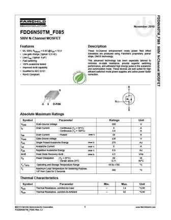
|Vds|ⓘ - Voltaje máximo drenador-fuente: 500 V
|Vgs|ⓘ - Voltaje máximo fuente-puerta: 30 V
|Id|ⓘ - Corriente continua de drenaje: 6 A
Tjⓘ - Temperatura máxima de unión: 150 °C
CARACTERÍSTICAS ELÉCTRICAS
trⓘ - Tiempo de subida: 55 nS
Cossⓘ - Capacitancia de salida: 95 pF
RDSonⓘ - Resistencia estado encendido drenaje a fuente: 0.9 Ohm
Encapsulados: D-PAK
📄📄 Copiar
Búsqueda de reemplazo de FDD6N50TM MOSFET
- Selecciónⓘ de transistores por parámetros
FDD6N50TM datasheet
fdd6n50tf fdd6n50tm fdu6n50 fdu6n50tu.pdf
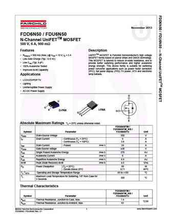
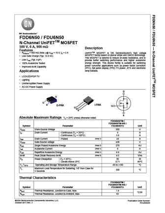
November 2013 FDD6N50 / FDU6N50 N-Channel UniFETTM MOSFET 500 V, 6 A, 900 m Features Description RDS(on) = 900 m (Max.) @ VGS = 10 V, ID = 3 A UniFETTM MOSFET is Fairchild Semiconductor s high voltage MOSFET family based on planar stripe and DMOS technology. Low Gate Charge (Typ. 12.8 nC) This MOSFET is tailored to reduce on-state resistance, and to Low Crss (Typ. 9 p
fdd6n50tm.pdf
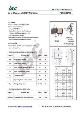
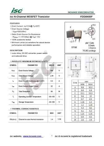
isc N-Channel MOSFET Transistor FDD6N50TM FEATURES Drain Current I =6A@ T =25 D C Drain Source Voltage V =500V(Min) DSS Static Drain-Source On-Resistance R =0.9 (Max) @ V = 10V DS(on) GS 100% avalanche tested Minimum Lot-to-Lot variations for robust device performance and reliable operation DESCRIPTION motor drive, DC-DC converter, power switch and solenoid
fdd6n50tm-f085.pdf
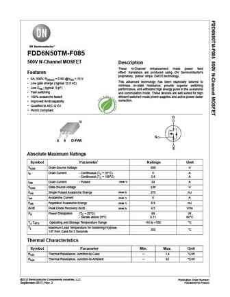
FDD6N50TM-F085 500V N-Channel MOSFET Description These N-Channel enhancement mode power field effect transistors are produced using ON Semiconductor's Features proprietary, planar stripe, DMOS technology. 6A, 500V, RDS(on) = 0.9 @VGS = 10 V This advanced technology has been especially tailored to Low gate charge ( typical 12.8 nC) minimize on-state resistance, provide s

Otros transistores... FDD6688S, FDD6696, FDD6776A, FDD6780, FDD6782A, FDD6796, FDD6N20TF, FDD6N50TF, IRFP250N, FDD7030BL, FDD7N25LZTM, FDD7N60NZTM, FDD8580, FDD8586, FDD86367F085, FDD86369F085, FDD8750
Parámetros del MOSFET. Cómo se afectan entre sí.
History: APT8024LFLLG | NTZD3155CT2G
🌐 : EN ES РУ

Liste
Recientemente añadidas las descripciónes de los transistores:
MOSFET: CS95118 | CS85105A | CS75N45 | CS72N12 | CS55N50 | CS48N75A | CS40N27 | MSQ60P04D | MSQ40P07D | MSQ30P40D | MSQ30P15 | MSQ30P07D | MSQ100N03D | MSHM60P14 | MSHM40N085 | MSHM30N46
Popular searches
2n2222a transistor | irfp250 | irf640n datasheet | irf540 datasheet | irf530 | 2n3565 | irf530n | pn2222a datasheet