FDFMA2P857 MOSFET Equivalente. Reemplazo. Hoja de especificaciones. Principales características
Número de Parte: FDFMA2P857
Tipo de FET: MOSFET
Polaridad de transistor: P
ESPECIFICACIONES MÁXIMAS
Pdⓘ - Máxima disipación de potencia: 1.4 W
|Vds|ⓘ - Voltaje máximo drenador-fuente: 20 V
|Vgs|ⓘ - Voltaje máximo fuente-puerta: 8 V
|Id|ⓘ - Corriente continua de drenaje: 3 A
Tjⓘ - Temperatura máxima de unión: 150 °C
CARACTERÍSTICAS ELÉCTRICAS
trⓘ - Tiempo de subida: 11 nS
Cossⓘ - Capacitancia de salida: 80 pF
RDSonⓘ - Resistencia estado encendido drenaje a fuente: 0.12 Ohm
Encapsulados: MICROFET2X2
Búsqueda de reemplazo de FDFMA2P857 MOSFET
- Selecciónⓘ de transistores por parámetros
FDFMA2P857 datasheet
fdfma2p857.pdf
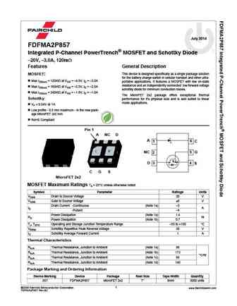
July 2014 FDFMA2P857 Integrated P-Channel PowerTrench MOSFET and Schottky Diode 20V, 3.0A, 120m Features General Description This device is designed specifically as a single package solution MOSFET for the battery charge switch in cellular handset and other ultra- Max rDS(on) = 120m at VGS = 4.5V, ID = 3.0A portable applications. It features a MOSFET with low on-s
fdfma2p853t.pdf
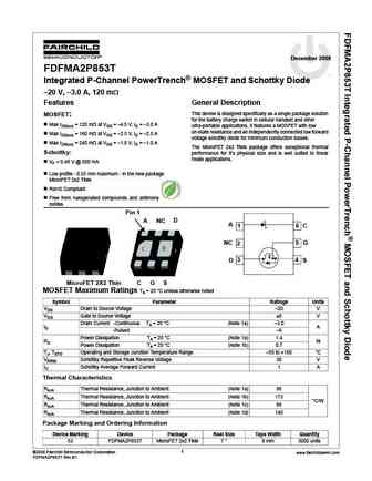
December 2008 FDFMA2P853T tm Integrated P-Channel PowerTrench MOSFET and Schottky Diode 20 V, 3.0 A, 120 m Features General Description This device is designed specifically as a single package solution MOSFET for the battery charge switch in cellular handset and other Max rDS(on) = 120 m at VGS = 4.5 V, ID = 3.0 A ultra-portable applications. It features a MOS
fdfma2p859t.pdf
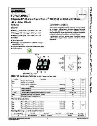
July 2009 FDFMA2P859T Integrated P-Channel PowerTrench MOSFET and Schottky Diode 20 V, 3.0 A, 120 m Features General Description This device is designed specifically as a single package solution MOSFET for the battery charge switch in cellular handset and other Max rDS(on) = 120 m at VGS = 4.5 V, ID = 3.0 A ultra-portable applications. It features a MOSFET with low
fdfma2p853.pdf
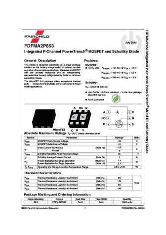
September 2008 July 2014 FDFMA2P853 Integrated P-Channel PowerTrench MOSFET and Schottky Diode General Description Features This device is designed specifically as a single package MOSFET solution for the battery charge switch in cellular handset -3.0 A, -20V. RDS(ON) = 120 m @ VGS = -4.5 V and other ultra-portable applications. It features a MOSFET with low on-state resis
Otros transistores... FDFC2P100, FDFC3N108, FDFM2N111, FDFM2P110, FDFMA2N028Z, FDFMA2P029Z, FDFMA2P853, FDFMA2P853T, 12N60, FDFMA2P859T, FDFMA3N109, FDFME2P823ZT, FDFME3N311ZT, FDFMJ2P023Z, FDFS2P102, FDFS2P102A, FDFS2P103
🌐 : EN ES РУ

Liste
Recientemente añadidas las descripciónes de los transistores:
MOSFET: CM4407 | CM3407 | CM3400 | SVF11N65F | SVF11N65T | FKBB3105 | EHBA036R1 | CRTT067N10N | AP6NA3R2MT | AP65SA145DDT8 | AP4NAR95CMT-A | AP4024GEMT-HF | AP3P050AH | AP3P020H | AP3N9R5YT | AP3N9R5MT
Popular searches
ksa992 | irfb4227 | irfb4110 | tip36c | bd139 transistor | irf840 datasheet | ge10001 | irf830