SFR9110TF Datasheet. Equivalente. Reemplazo. Hoja de especificaciones. Principales características
Número de Parte: SFR9110TF 📄📄
Tipo de FET: MOSFET
Polaridad de transistor: P
ESPECIFICACIONES MÁXIMAS
Pdⓘ - Máxima disipación de potencia: 20 W
|Vds|ⓘ - Voltaje máximo drenador-fuente: 100 V
|Vgs|ⓘ - Voltaje máximo fuente-puerta: 30 V
|Id|ⓘ - Corriente continua de drenaje: 2.8 A
Tjⓘ - Temperatura máxima de unión: 150 °C
CARACTERÍSTICAS ELÉCTRICAS
trⓘ - Tiempo de subida: 20 nS
Cossⓘ - Capacitancia de salida: 50 pF
RDSonⓘ - Resistencia estado encendido drenaje a fuente: 1.2 Ohm
Encapsulados: DPAK
Búsqueda de reemplazo de SFR9110TF MOSFET
- Selecciónⓘ de transistores por parámetros
SFR9110TF datasheet
sfr9110tf.pdf
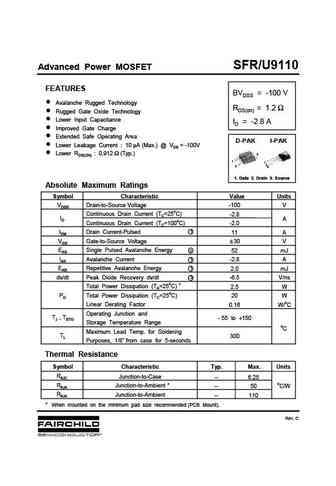
SFR/U9110 Advanced Power MOSFET FEATURES BVDSS = -100 V n Avalanche Rugged Technology RDS(on) = 1.2 n Rugged Gate Oxide Technology n Lower Input Capacitance ID = -2.8 A n Improved Gate Charge n Extended Safe Operating Area D-PAK I-PAK n Lower Leakage Current 10 A(Max.) @ VDS = -100V n Lower RDS(ON) 0.912 (Typ.) 2 1 1 2 3 3 1. Gate 2. Drain 3. Source Absolute M
sfu9110 sfr9110.pdf

SFR/U9110 Advanced Power MOSFET FEATURES BVDSS = -100 V n Avalanche Rugged Technology RDS(on) = 1.2 n Rugged Gate Oxide Technology n Lower Input Capacitance ID = -2.8 A n Improved Gate Charge n Extended Safe Operating Area D-PAK I-PAK n Lower Leakage Current 10 A(Max.) @ VDS = -100V n Lower RDS(ON) 0.912 (Typ.) 2 1 1 2 3 3 1. Gate 2. Drain 3. Source Absolute M
sfr9110.pdf
Advanced Power MOSFET FEATURES BVDSS = -100 V Avalanche Rugged Technology RDS(on) = 1.2 Rugged Gate Oxide Technology Lower Input Capacitance ID = -2.8 A Improved Gate Charge Extended Safe Operating Area Lower Leakage Current 10 A (Max.) @ VDS = -100V Lower RDS(ON) 0.912 (Typ.) 2 1 1 2 3 3 1. Gate 2. Drain 3. Source Absolute Maximum Ratings Symbol Chara
sfu9130 sfr9130.pdf
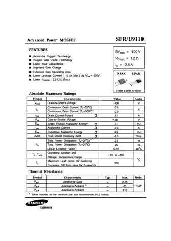
SFR/U9130 Advanced Power MOSFET FEATURES BVDSS = -100 V Avalanche Rugged Technology RDS(on) = 0.3 Rugged Gate Oxide Technology Lower Input Capacitance ID = -9.8 A Improved Gate Charge Extended Safe Operating Area D-PAK I-PAK Lower Leakage Current 10 A (Max.) @ VDS = -100V Lower RDS(ON) 0.225 (Typ.) 2 1 1 2 3 3 1. Gate 2. Drain 3. Source Absolute Maximum


Otros transistores... SFP830, SFP830D, SFP840, SFP9640L, SFP9N50, SFR9014TF, SFR9024TM, SFR9034TF, AOD4184A, SFT1452, SFT210DE, SFT6661, SFW9530TM, SFW9640TM, SFW9Z34TM, SQM100N04-2M7, SQM100N04-3M5
🌐 : EN ES РУ

Liste
Recientemente añadidas las descripciónes de los transistores:
MOSFET: ASDM30DN30E | ASDM3050KQ | ASDM2305 | ASDM2301 | ASDM2300ZA | ASDM20P13S | ASDM20N90Q | ASDM20N60 | ASDM7002EZA | ASDM68N80KQ | ASDM6802ZC | ASDM60R042NQ | ASDM60P12KQ | ASDM60N80KQ | ASDM60N70Q | ASDM60N50KQ
Popular searches
2n3567 | 2sc1226 | 2sd180 | 2sd235 | k3502 datasheet | p0903bdg datasheet | 2sa722 | f1010e mosfet datasheet