SFR9110TF Datasheet. Specs and Replacement
Type Designator: SFR9110TF 📄📄
Type of Transistor: MOSFET
Type of Control Channel: P-Channel
Absolute Maximum Ratings
Pd ⓘ - Maximum Power Dissipation: 20 W
|Vds|ⓘ - Maximum Drain-Source Voltage: 100 V
|Vgs|ⓘ - Maximum Gate-Source Voltage: 30 V
|Id| ⓘ - Maximum Drain Current: 2.8 A
Tj ⓘ - Maximum Junction Temperature: 150 °C
Electrical Characteristics
tr ⓘ - Rise Time: 20 nS
Cossⓘ - Output Capacitance: 50 pF
RDSonⓘ - Maximum Drain-Source On-State Resistance: 1.2 Ohm
Package: DPAK
📄📄 Copy
SFR9110TF substitution
- MOSFET ⓘ Cross-Reference Search
SFR9110TF datasheet
sfr9110tf.pdf
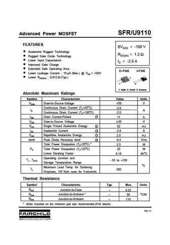
SFR/U9110 Advanced Power MOSFET FEATURES BVDSS = -100 V n Avalanche Rugged Technology RDS(on) = 1.2 n Rugged Gate Oxide Technology n Lower Input Capacitance ID = -2.8 A n Improved Gate Charge n Extended Safe Operating Area D-PAK I-PAK n Lower Leakage Current 10 A(Max.) @ VDS = -100V n Lower RDS(ON) 0.912 (Typ.) 2 1 1 2 3 3 1. Gate 2. Drain 3. Source Absolute M... See More ⇒
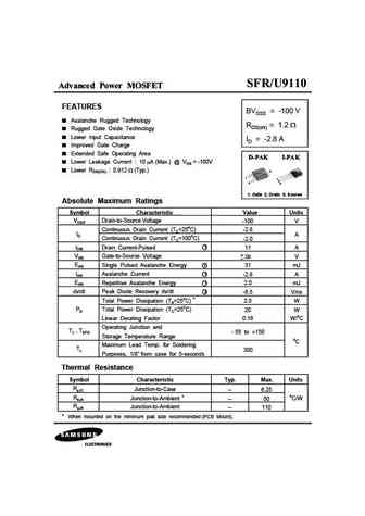
sfu9110 sfr9110.pdf

SFR/U9110 Advanced Power MOSFET FEATURES BVDSS = -100 V n Avalanche Rugged Technology RDS(on) = 1.2 n Rugged Gate Oxide Technology n Lower Input Capacitance ID = -2.8 A n Improved Gate Charge n Extended Safe Operating Area D-PAK I-PAK n Lower Leakage Current 10 A(Max.) @ VDS = -100V n Lower RDS(ON) 0.912 (Typ.) 2 1 1 2 3 3 1. Gate 2. Drain 3. Source Absolute M... See More ⇒
sfr9110.pdf
Advanced Power MOSFET FEATURES BVDSS = -100 V Avalanche Rugged Technology RDS(on) = 1.2 Rugged Gate Oxide Technology Lower Input Capacitance ID = -2.8 A Improved Gate Charge Extended Safe Operating Area Lower Leakage Current 10 A (Max.) @ VDS = -100V Lower RDS(ON) 0.912 (Typ.) 2 1 1 2 3 3 1. Gate 2. Drain 3. Source Absolute Maximum Ratings Symbol Chara... See More ⇒
sfu9130 sfr9130.pdf
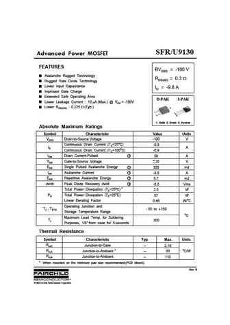
SFR/U9130 Advanced Power MOSFET FEATURES BVDSS = -100 V Avalanche Rugged Technology RDS(on) = 0.3 Rugged Gate Oxide Technology Lower Input Capacitance ID = -9.8 A Improved Gate Charge Extended Safe Operating Area D-PAK I-PAK Lower Leakage Current 10 A (Max.) @ VDS = -100V Lower RDS(ON) 0.225 (Typ.) 2 1 1 2 3 3 1. Gate 2. Drain 3. Source Absolute Maximum... See More ⇒


Detailed specifications: SFP830, SFP830D, SFP840, SFP9640L, SFP9N50, SFR9014TF, SFR9024TM, SFR9034TF, 75N75, SFT1452, SFT210DE, SFT6661, SFW9530TM, SFW9640TM, SFW9Z34TM, SQM100N04-2M7, SQM100N04-3M5
Keywords - SFR9110TF MOSFET specs
SFR9110TF cross reference
SFR9110TF equivalent finder
SFR9110TF pdf lookup
SFR9110TF substitution
SFR9110TF replacement
Can't find your MOSFET? Learn how to find a substitute transistor by analyzing voltage, current and package compatibility
MOSFET Parameters. How They Affect Each Other
History: AGM025N10C | NCE50NF180D | IRF830I-HF | PK5C1BA | KF15N50N | SM6018NSKP | AGM304A
🌐 : EN ES РУ

LIST
Last Update
MOSFET: CS95118 | CS85105A | CS75N45 | CS72N12 | CS55N50 | CS48N75A | CS40N27 | MSQ60P04D | MSQ40P07D | MSQ30P40D
Popular searches
2n3567 | 2sc1226 | 2sd180 | 2sd235 | k3502 datasheet | p0903bdg datasheet | 2sa722 | f1010e mosfet datasheet