SFW9Z34TM Datasheet. Specs and Replacement
Type Designator: SFW9Z34TM 📄📄
Type of Transistor: MOSFET
Type of Control Channel: P-Channel
Absolute Maximum Ratings
Pd ⓘ - Maximum Power Dissipation: 82 W
|Vds|ⓘ - Maximum Drain-Source Voltage: 60 V
|Vgs|ⓘ - Maximum Gate-Source Voltage: 30 V
|Id| ⓘ - Maximum Drain Current: 18 A
Tj ⓘ - Maximum Junction Temperature: 175 °C
Electrical Characteristics
tr ⓘ - Rise Time: 24 nS
Cossⓘ - Output Capacitance: 265 pF
RDSonⓘ - Maximum Drain-Source On-State Resistance: 0.14 Ohm
Package: D2PAK
SFW9Z34TM substitution
- MOSFET ⓘ Cross-Reference Search
SFW9Z34TM datasheet
sfw9z34tm.pdf
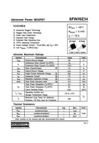
SFW/I9Z34 Advanced Power MOSFET FEATURES BVDSS = -60 V Avalanche Rugged Technology RDS(on) = 0.14 Rugged Gate Oxide Technology Lower Input Capacitance ID = -18 A Improved Gate Charge Extended Safe Operating Area D2-PAK I2-PAK 175oC Operating Temperature 2 Lower Leakage Current 10 A(Max.) @ VDS = -60V Low RDS(ON) 0.106 (Typ.) 1 1 2 3 3 1. Gate 2. Drain... See More ⇒
sfw9z34.pdf

Advanced Power MOSFET FEATURES BVDSS = -60 V Avalanche Rugged Technology RDS(on) = 0.14 Rugged Gate Oxide Technology Lower Input Capacitance ID = -18 A Improved Gate Charge Extended Safe Operating Area 175oC Operating Temperature 2 Lower Leakage Current 10 A (Max.) @ VDS = -60V Low RDS(ON) 0.106 (Typ.) 1 1 2 3 3 1. Gate 2. Drain 3. Source Absolute... See More ⇒
sfi9z24 sfw9z24.pdf

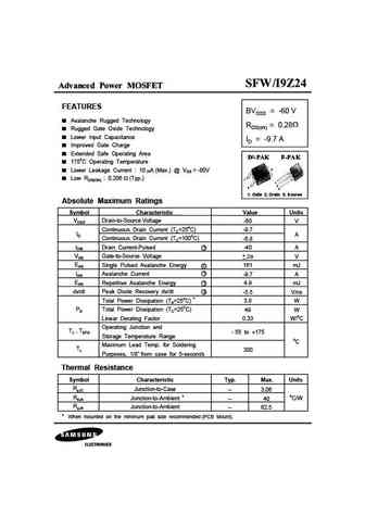
SFW/I9Z24 Advanced Power MOSFET FEATURES BVDSS = -60 V n Avalanche Rugged Technology RDS(on) = 0.28 n Rugged Gate Oxide Technology n Lower Input Capacitance ID = -9.7 A n Improved Gate Charge n Extended Safe Operating Area D2-PAK I2-PAK n 175oC Operating Temperature 2 n Lower Leakage Current 10 A(Max.) @ VDS = -60V n Low RDS(ON) 0.206 (Typ.) 1 1 2 3 3 1. Gate ... See More ⇒
sfi9z14 sfw9z14.pdf
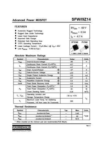
SFW/I9Z14 Advanced Power MOSFET FEATURES BVDSS = -60 V n Avalanche Rugged Technology RDS(on) = 0.5 n Rugged Gate Oxide Technology n Lower Input Capacitance ID = -6.7 A n Improved Gate Charge n Extended Safe Operating Area D2-PAK I2-PAK n 175oC Operating Temperature 2 n Lower Leakage Current 10 A(Max.) @ VDS = -60V n Low RDS(ON) 0.362 (Typ.) 1 1 2 3 3 1. Gate... See More ⇒

Detailed specifications: SFR9024TM, SFR9034TF, SFR9110TF, SFT1452, SFT210DE, SFT6661, SFW9530TM, SFW9640TM, IRFZ44N, SQM100N04-2M7, SQM100N04-3M5, SQM100N10-10, SQM110N04-02L, SQM110N04-03, SQM110N04-03L, SQM110N04-04, SQM110N05-06L
Keywords - SFW9Z34TM MOSFET specs
SFW9Z34TM cross reference
SFW9Z34TM equivalent finder
SFW9Z34TM pdf lookup
SFW9Z34TM substitution
SFW9Z34TM replacement
Learn how to find the right MOSFET substitute. A guide to cross-reference, check specs and replace MOSFETs in your circuits.
History: HFP2N60F | SQM100N04-2M7 | HFP5N60F
🌐 : EN ES РУ

LIST
Last Update
MOSFET: ASDM30P100KQ | ASDM30N90Q | ASDM30N75KQ | ASDM30N150Q | ASDM30N120Q | ASDM30N120KQ | ASDM30N100KQ | ASDM30DN40E | ASDM30DN30E | ASDM3050KQ
Popular searches
2sa722 | f1010e mosfet datasheet | 2sa566 | bc559 equivalent | c2075 transistor | ecg123 | 2n5551 transistor equivalent | 13009 datasheet