TK10A80E Datasheet. Equivalente. Reemplazo. Hoja de especificaciones. Principales características
Número de Parte: TK10A80E 📄📄
Tipo de FET: MOSFET
Polaridad de transistor: N
ESPECIFICACIONES MÁXIMAS
Pdⓘ - Máxima
disipación de potencia: 50 W
|Vds|ⓘ - Voltaje máximo drenador-fuente: 800 V
|Vgs|ⓘ - Voltaje máximo fuente-puerta: 30 V
|Id|ⓘ - Corriente continua
de drenaje: 10 A
Tjⓘ - Temperatura máxima de unión: 150 °C
CARACTERÍSTICAS ELÉCTRICAS
trⓘ - Tiempo
de subida: 40 nS
Cossⓘ - Capacitancia de salida: 150 pF
RDSonⓘ - Resistencia estado encendido drenaje a fuente: 1 Ohm
Encapsulados: TO-220SIS
Búsqueda de reemplazo de TK10A80E MOSFET
- Selecciónⓘ de transistores por parámetros
TK10A80E datasheet
..1. Size:218K toshiba
tk10a80e.pdf 
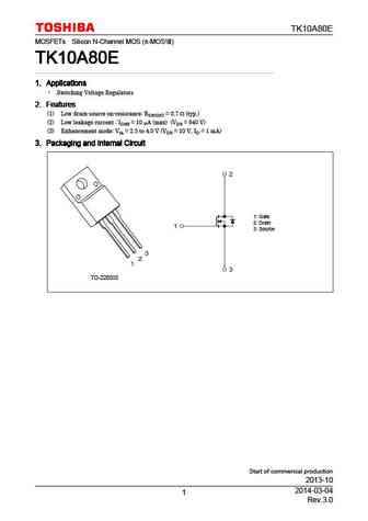
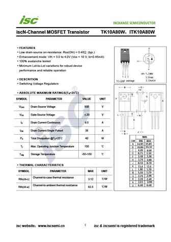
TK10A80E MOSFETs Silicon N-Channel MOS ( -MOS ) TK10A80E TK10A80E TK10A80E TK10A80E 1. Applications 1. Applications 1. Applications 1. Applications Switching Voltage Regulators 2. Features 2. Features 2. Features 2. Features (1) Low drain-source on-resistance RDS(ON) = 0.7 (typ.) (2) Low leakage current IDSS = 10 A (max) (VDS = 640 V) (3) Enhancement mode Vth =
..2. Size:239K inchange semiconductor
tk10a80e.pdf
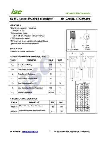
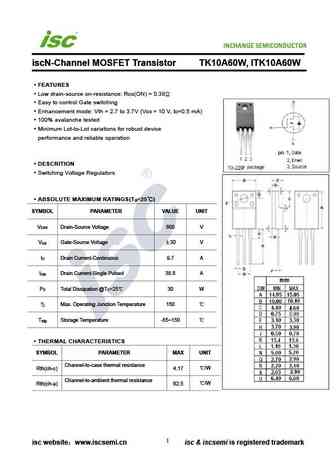
INCHANGE Semiconductor isc N-Channel MOSFET Transistor TK10A80E ITK10A80E FEATURES Low drain-source on-resistance RDS(on) 1.0 . Enhancement mode Vth = 2.5 to4.0V (VDS = 10 V, ID=1.0mA) 100% avalanche tested Minimum Lot-to-Lot variations for robust device performance and reliable operation DESCRITION Switching Voltage Regulators ABSOLUTE MAXIMUM RATINGS(T =25
7.1. Size:412K toshiba
tk10a80w.pdf
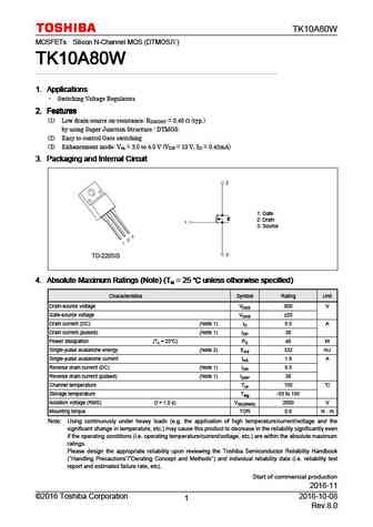
TK10A80W MOSFETs Silicon N-Channel MOS (DTMOS ) TK10A80W TK10A80W TK10A80W TK10A80W 1. Applications 1. Applications 1. Applications 1. Applications Switching Voltage Regulators 2. Features 2. Features 2. Features 2. Features (1) Low drain-source on-resistance RDS(ON) = 0.46 (typ.) by using Super Junction Structure DTMOS (2) Easy to control Gate switching (3) Enhan
7.2. Size:253K inchange semiconductor
tk10a80w.pdf
INCHANGE Semiconductor iscN-Channel MOSFET Transistor TK10A80W ITK10A80W FEATURES Low drain-source on-resistance RDS(ON) = 0.46 (typ.) Enhancement mode Vth = 3.0 to 4.0V (VDS = 10 V, ID=0.45mA) 100% avalanche tested Minimum Lot-to-Lot variations for robust device performance and reliable operation DESCRITION Switching Voltage Regulators ABSOLUTE MAXIMUM RATINGS(
9.1. Size:248K toshiba
tk10a60d.pdf
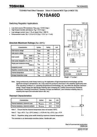
TK10A60D TOSHIBA Field Effect Transistor Silicon N Channel MOS Type ( -MOS VII) TK10A60D Unit mm Switching Regulator Applications Low drain-source ON-resistance RDS (ON) = 0.58 (typ.) High forward transfer admittance Yfs = 6.0 S (typ.) Low leakage current IDSS = 10 A (max) (VDS = 600 V) Enhancement mode Vth = 2.0 to 4.0 V (VDS = 10 V, ID = 1 mA) A
9.2. Size:189K toshiba
tk10a55d.pdf
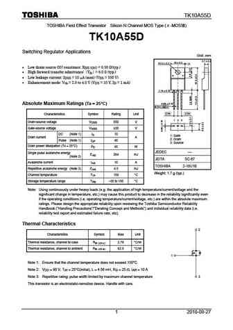
TK10A55D TOSHIBA Field Effect Transistor Silicon N Channel MOS Type ( -MOS ) TK10A55D Switching Regulator Applications Unit mm 2.7 0.2 10 0.3 3.2 0.2 A Low drain-source ON-resistance RDS (ON) = 0.56 (typ.) High forward transfer admittance Yfs = 6.0 S (typ.) Low leakage current IDSS = 10 A (max) (VDS = 550 V) Enhancement mode Vth
9.3. Size:240K toshiba
tk10a60w.pdf
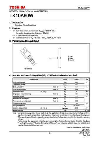
TK10A60W MOSFETs Silicon N-Channel MOS (DTMOS ) TK10A60W TK10A60W TK10A60W TK10A60W 1. Applications 1. Applications 1. Applications 1. Applications Switching Voltage Regulators 2. Features 2. Features 2. Features 2. Features (1) Low drain-source on-resistance RDS(ON) = 0.327 (typ.) by used to Super Junction Structure DTMOS (2) Easy to control Gate switching (3) E
9.4. Size:238K toshiba
tk10a60w5.pdf
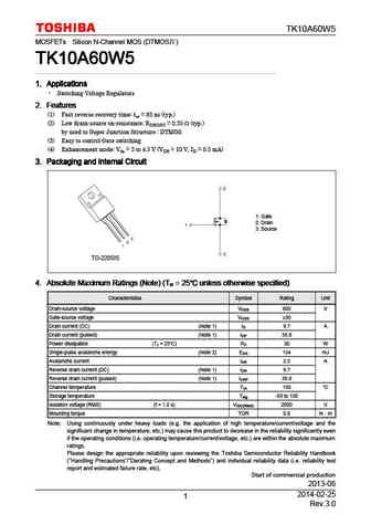
TK10A60W5 MOSFETs Silicon N-Channel MOS (DTMOS ) TK10A60W5 TK10A60W5 TK10A60W5 TK10A60W5 1. Applications 1. Applications 1. Applications 1. Applications Switching Voltage Regulators 2. Features 2. Features 2. Features 2. Features (1) Fast reverse recovery time trr = 85 ns (typ.) (2) Low drain-source on-resistance RDS(ON) = 0.35 (typ.) by used to Super Junction Stru
9.5. Size:245K toshiba
tk10a60d5.pdf
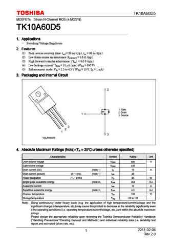
TK10A60D5 MOSFETs Silicon N-Channel MOS ( -MOS ) TK10A60D5 TK10A60D5 TK10A60D5 TK10A60D5 1. Applications 1. Applications 1. Applications 1. Applications Switching Voltage Regulators 2. Features 2. Features 2. Features 2. Features (1) Fast reverse recovery time trrf = 50 ns (typ.), trr = 90 ns (typ.) (2) Low drain-source on-resistance RDS(ON) = 0.8 (typ.) (3) High f
9.6. Size:197K toshiba
tk10a50d.pdf
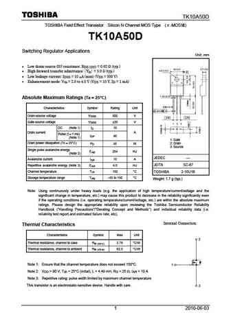
TK10A50D TOSHIBA Field Effect Transistor Silicon N Channel MOS Type ( -MOS ) TK10A50D Switching Regulator Applications Unit mm Low drain-source ON-resistance RDS (ON) = 0.62 (typ.) High forward transfer admittance Yfs = 5.0 S (typ.) Low leakage current IDSS = 10 A (max) (VDS = 500 V) Enhancement mode Vth = 2.0 to 4.0 V (VDS = 10 V, ID = 1 mA)
9.7. Size:251K toshiba
tk10a50w.pdf

TK10A50W MOSFETs Silicon N-Channel MOS (DTMOS ) TK10A50W TK10A50W TK10A50W TK10A50W 1. Applications 1. Applications 1. Applications 1. Applications Switching Voltage Regulators 2. Features 2. Features 2. Features 2. Features (1) Low drain-source on-resistance RDS(ON) = 0.327 (typ.) by used to Super Junction Structure DTMOS (2) Easy to control Gate switching (3) E
9.8. Size:253K inchange semiconductor
tk10a60d.pdf

INCHANGE Semiconductor iscN-Channel MOSFET Transistor TK10A60D ITK10A60D FEATURES Low drain-source on-resistance RDS(ON) = 0.58 (typ.) Enhancement mode Vth = 2.0 to 4.0V (VDS = 10 V, ID=1.0mA) 100% avalanche tested Minimum Lot-to-Lot variations for robust device performance and reliable operation DESCRITION Switching Voltage Regulators ABSOLUTE MAXIMUM RATINGS
9.9. Size:252K inchange semiconductor
tk10a55d.pdf
INCHANGE Semiconductor iscN-Channel MOSFET Transistor TK10A55D ITK10A55D FEATURES Low drain-source on-resistance RDS(ON) = 0.56 (typ.) Enhancement mode Vth = 2.0 to 4.0V (VDS = 10 V, ID=1.0mA) 100% avalanche tested Minimum Lot-to-Lot variations for robust device performance and reliable operation DESCRITION Switching Voltage Regulators ABSOLUTE MAXIMUM RATINGS
9.11. Size:253K inchange semiconductor
tk10a60w5.pdf
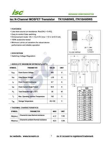
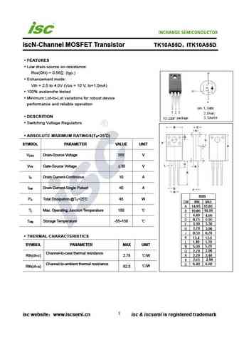
INCHANGE Semiconductor isc N-Channel MOSFET Transistor TK10A60W5, lTK10A60W5 FEATURES Low drain-source on-resistance RDS(ON) = 0.45 Easy to control Gate switching Enhancement mode Vth = 3 to 4.5V (VDS = 10 V, ID=0.5 mA) 100% avalanche tested Minimum Lot-to-Lot variations for robust device performance and reliable operation DESCRITION Switching Voltage Regulators
9.12. Size:252K inchange semiconductor
tk10a60d5.pdf
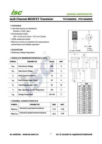
INCHANGE Semiconductor iscN-Channel MOSFET Transistor TK10A60D5 ITK10A60D5 FEATURES Low drain-source on-resistance RDS(on) = 0.8 (typ.) Enhancement mode Vth = 2.5 to 4.5V (VDS = 10 V, ID=1.0mA) 100% avalanche tested Minimum Lot-to-Lot variations for robust device performance and reliable operation DESCRITION Switching Voltage Regulators ABSOLUTE MAXIMUM RATING
9.13. Size:252K inchange semiconductor
tk10a50d.pdf
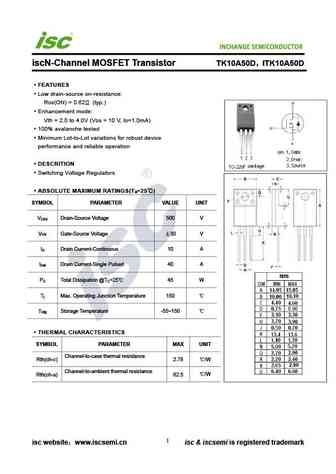
INCHANGE Semiconductor iscN-Channel MOSFET Transistor TK10A50D ITK10A50D FEATURES Low drain-source on-resistance RDS(ON) = 0.62 (typ.) Enhancement mode Vth = 2.0 to 4.0V (VDS = 10 V, ID=1.0mA) 100% avalanche tested Minimum Lot-to-Lot variations for robust device performance and reliable operation DESCRITION Switching Voltage Regulators ABSOLUTE MAXIMUM RATINGS
9.14. Size:253K inchange semiconductor
tk10a50w.pdf
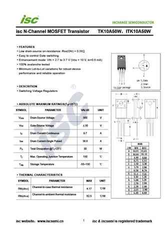
INCHANGE Semiconductor isc N-Channel MOSFET Transistor TK10A50W ITK10A50W FEATURES Low drain-source on-resistance RDS(ON) = 0.38 Easy to control Gate switching Enhancement mode Vth = 2.7 to 3.7 V (VDS = 10 V, ID=0.5 mA) 100% avalanche tested Minimum Lot-to-Lot variations for robust device performance and reliable operation DESCRITION Switching Voltage Regulators
Otros transistores... TK100A08N1, TK100A10N1, TK100E06N1, TK100E08N1, TK100E10N1, TK100L60W, TK100S04N1L, TK10A60W5, IRFZ44N, TK10E60W, TK10J80E, TK10P60W, TK10Q60W, TK10V60W, TK11A65W, TK11P65W, TK11Q65W