TK40A06N1 MOSFET Equivalente. Reemplazo. Hoja de especificaciones. Principales características
Número de Parte: TK40A06N1
Tipo de FET: MOSFET
Polaridad de transistor: N
ESPECIFICACIONES MÁXIMAS
Pdⓘ - Máxima disipación de potencia: 30 W
|Vds|ⓘ - Voltaje máximo drenador-fuente: 60 V
|Vgs|ⓘ - Voltaje máximo fuente-puerta: 20 V
|Id|ⓘ - Corriente continua de drenaje: 40 A
Tjⓘ - Temperatura máxima de unión: 150 °C
CARACTERÍSTICAS ELÉCTRICAS
trⓘ - Tiempo de subida: 14 nS
Cossⓘ - Capacitancia de salida: 580 pF
RDSonⓘ - Resistencia estado encendido drenaje a fuente: 0.0104 Ohm
Encapsulados: TO-220SIS
Búsqueda de reemplazo de TK40A06N1 MOSFET
- Selecciónⓘ de transistores por parámetros
TK40A06N1 datasheet
tk40a06n1.pdf
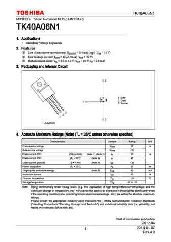
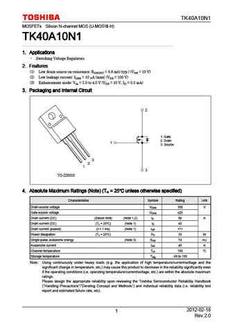
TK40A06N1 MOSFETs Silicon N-channel MOS (U-MOS -H) TK40A06N1 TK40A06N1 TK40A06N1 TK40A06N1 1. Applications 1. Applications 1. Applications 1. Applications Switching Voltage Regulators 2. Features 2. Features 2. Features 2. Features (1) Low drain-source on-resistance RDS(ON) = 8.4 m (typ.) (VGS = 10 V) (2) Low leakage current IDSS = 10 A (max) (VDS = 60 V) (3) Enhan
tk40a06n1.pdf
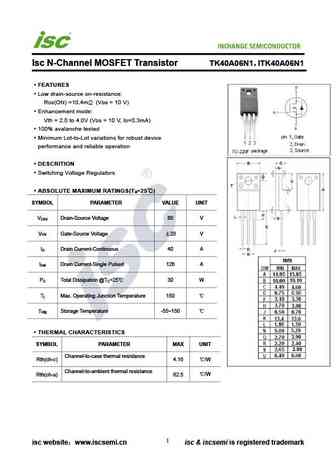
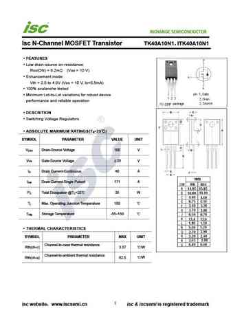
INCHANGE Semiconductor Isc N-Channel MOSFET Transistor TK40A06N1 ITK40A06N1 FEATURES Low drain-source on-resistance RDS(ON) =10.4m (VGS = 10 V) Enhancement mode Vth = 2.0 to 4.0V (VDS = 10 V, ID=0.3mA) 100% avalanche tested Minimum Lot-to-Lot variations for robust device performance and reliable operation DESCRITION Switching Voltage Regulators ABSOLUTE MAXI
tk40a10j1.pdf
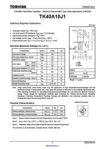
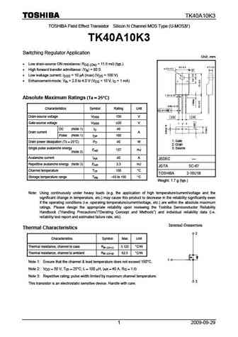
TK40A10J1 TOSHIBA Field Effect Transistor Silicon N Channel MOS Type (Ultra-High-Speed U-MOS ) TK40A10J1 Switching Regulator Applications Unit mm Small gate charge Qg = 76nC (typ.) Low drain-source ON-resistance RDS (ON) = 11.5 m (typ.) High forward transfer admittance Yfs = 90 S Low leakage current IDSS = 10 A (max) (VDS = 100 V) Enhancement m
Otros transistores... TK35N65W5 , TK39A60W , TK39J60W , TK39J60W5 , TK39N60W , TK39N60W5 , TK39N60X , TK3P80E , IRFZ44 , TK40E06N1 , TK40S06N1L , TK42A12N1 , TK42E12N1 , TK45S06K3L , TK46A08N1 , TK46E08N1 , TK49N65W .
🌐 : EN ES РУ

Liste
Recientemente añadidas las descripciónes de los transistores:
MOSFET: AUB062N08BG | AUB060N08AG | AUB056N10 | AUB056N08BGL | AUB050N085 | AUB050N055 | AUB045N12 | AUB045N10BT | AUB039N10 | AUB034N10 | AUB033N08BG | AUB026N085 | AUA062N08BG | AUA060N08AG | AUA056N08BGL | AUA039N10
Popular searches
irf640n datasheet | irf540 datasheet | irf530 | 2n3565 | irf530n | pn2222a datasheet | tip41c transistor | 2n5087