IRFW620A MOSFET Equivalente. Reemplazo. Hoja de especificaciones. Principales características
Número de Parte: IRFW620A
Tipo de FET: MOSFET
Polaridad de transistor: N
ESPECIFICACIONES MÁXIMAS
Pdⓘ - Máxima
disipación de potencia: 47 W
|Vds|ⓘ - Voltaje máximo drenador-fuente: 200 V
|Vgs|ⓘ - Voltaje máximo fuente-puerta: 30 V
|Id|ⓘ - Corriente continua
de drenaje: 5 A
Tjⓘ - Temperatura máxima de unión: 150 °C
CARACTERÍSTICAS ELÉCTRICAS
trⓘ - Tiempo
de subida: 11 nS
Cossⓘ - Capacitancia de salida: 55 pF
RDSonⓘ - Resistencia estado encendido drenaje a fuente: 0.8 Ohm
Encapsulados: TO263
Búsqueda de reemplazo de IRFW620A MOSFET
- Selecciónⓘ de transistores por parámetros
IRFW620A datasheet
8.2. Size:514K samsung
irfw624a.pdf 

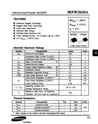
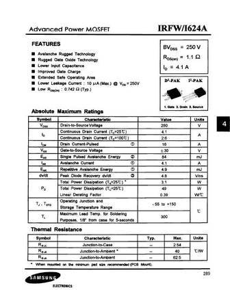
Advanced Power MOSFET FEATURES BVDSS = 250 V Avalanche Rugged Technology RDS(on) = 1.1 Rugged Gate Oxide Technology Lower Input Capacitance ID = 4.1 A Improved Gate Charge Extended Safe Operating Area Lower Leakage Current 10 A (Max.) @ VDS = 250V 2 Low RDS(ON) 0.742 (Typ.) 1 1 2 3 3 1. Gate 2. Drain 3. Source Absolute Maximum Ratings Symbol Chara
9.7. Size:712K fairchild semi
irfw630b irfi630b.pdf
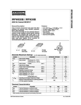
IRFW630B / IRFI630B 200V N-Channel MOSFET General Description Features These N-Channel enhancement mode power field effect 9.0A, 200V, RDS(on) = 0.4 @VGS = 10 V transistors are produced using Fairchild s proprietary, Low gate charge ( typical 22 nC) planar, DMOS technology. Low Crss ( typical 22 pF) This advanced technology has been especially tailored to Fast switc
9.8. Size:697K fairchild semi
irfw630b.pdf
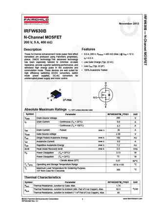
November 2013 IRFW630B N-Channel MOSFET 200 V, 9 A, 400 m Features Description These N-Channel enhancement mode power field effect 9.0 A, 200 V, RDS(on) = 400 m (Max.) @ VGS = 10 V, transistors are produced using Fairchild s proprietary, ID = 4.5 A planar, DMOS technology.This advanced technology has been especially tailored to minimize on-state Low Gate Charge (Typ.
9.9. Size:798K fairchild semi
irfw610b irfi610b.pdf

November 2001 IRFW610B / IRFI610B 200V N-Channel MOSFET General Description Features These N-Channel enhancement mode power field effect 3.3A, 200V, RDS(on) = 1.5 @VGS = 10 V transistors are produced using Fairchild s proprietary, Low gate charge ( typical 7.2 nC) planar, DMOS technology. Low Crss ( typical 6.8 pF) This advanced technology has been especially tailored t
9.10. Size:509K samsung
irfw630a.pdf

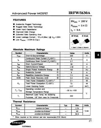
Advanced Power MOSFET FEATURES BVDSS = 200 V Avalanche Rugged Technology RDS(on) = 0.4 Rugged Gate Oxide Technology Lower Input Capacitance ID = 9 A Improved Gate Charge Extended Safe Operating Area Lower Leakage Current 10 A (Max.) @ VDS = 200V 2 Low RDS(ON) 0.333 (Typ.) 1 1 2 3 3 1. Gate 2. Drain 3. Source Absolute Maximum Ratings Symbol Charact
9.11. Size:505K samsung
irfw610a.pdf

Advanced Power MOSFET FEATURES BVDSS = 200 V Avalanche Rugged Technology RDS(on) = 1.5 Rugged Gate Oxide Technology Lower Input Capacitance ID = 3.3 A Improved Gate Charge Extended Safe Operating Area Lower Leakage Current 10 A (Max.) @ VDS = 200V 2 Low RDS(ON) 1.169 (Typ.) 1 1 2 3 3 1. Gate 2. Drain 3. Source Absolute Maximum Ratings Symbol Chara
9.12. Size:506K samsung
irfw644a.pdf

Advanced Power MOSFET FEATURES BVDSS = 250 V Avalanche Rugged Technology RDS(on) = 0.28 Rugged Gate Oxide Technology Lower Input Capacitance ID = 14 A Improved Gate Charge Extended Safe Operating Area Lower Leakage Current 10 A (Max.) @ VDS = 250V 2 Lower RDS(ON) 0.214 (Typ.) 1 1 2 3 3 1. Gate 2. Drain 3. Source Absolute Maximum Ratings Symbol Charact
9.13. Size:513K samsung
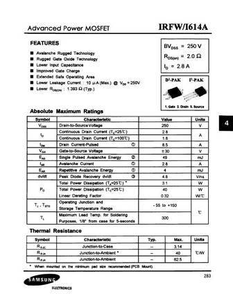
irfw614a.pdf
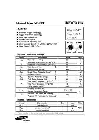
Advanced Power MOSFET FEATURES BVDSS = 250 V Avalanche Rugged Technology RDS(on) = 2.0 Rugged Gate Oxide Technology Lower Input Capacitance ID = 2.8 A Improved Gate Charge Extended Safe Operating Area Lower Leakage Current 10 A (Max.) @ VDS = 250V 2 Lower RDS(ON) 1.393 (Typ.) 1 1 2 3 3 1. Gate 2. Drain 3. Source Absolute Maximum Ratings Symbol Cha
9.14. Size:512K samsung
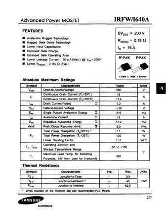
irfw640a.pdf

Advanced Power MOSFET FEATURES BVDSS = 200 V Avalanche Rugged Technology RDS(on) = 0.18 Rugged Gate Oxide Technology Lower Input Capacitance ID = 18 A Improved Gate Charge Extended Safe Operating Area Lower Leakage Current 10 A (Max.) @ VDS = 200V 2 Lower RDS(ON) 0.144 (Typ.) 1 1 2 3 3 1. Gate 2. Drain 3. Source Absolute Maximum Ratings Symbol Cha
Otros transistores... IRFW450
, IRFW510A
, IRFW520A
, IRFW530A
, IRFW540A
, IRFW550A
, IRFW610A
, IRFW614A
, IRF630
, IRFW624A
, IRFW630A
, IRFW634A
, IRFW640A
, IRFW644A
, IRFW710A
, IRFW720A
, IRFW730A
.