STP26NM60ND MOSFET Equivalente. Reemplazo. Hoja de especificaciones. Principales características
Número de Parte: STP26NM60ND
Tipo de FET: MOSFET
Polaridad de transistor: N
ESPECIFICACIONES MÁXIMAS
Pdⓘ - Máxima disipación de potencia: 190 W
|Vds|ⓘ - Voltaje máximo drenador-fuente: 600 V
|Vgs|ⓘ - Voltaje máximo fuente-puerta: 25 V
|Id|ⓘ - Corriente continua de drenaje: 21 A
Tjⓘ - Temperatura máxima de unión: 150 °C
CARACTERÍSTICAS ELÉCTRICAS
trⓘ - Tiempo de subida: 14.5 nS
Cossⓘ - Capacitancia de salida: 90 pF
RDSonⓘ - Resistencia estado encendido drenaje a fuente: 0.175 Ohm
Encapsulados: TO-220
Búsqueda de reemplazo de STP26NM60ND MOSFET
- Selecciónⓘ de transistores por parámetros
STP26NM60ND datasheet
stb26nm60nd stf26nm60nd stp26nm60nd stw26nm60nd.pdf
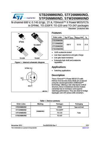
STB26NM60ND, STF26NM60ND, STP26NM60ND, STW26NM60ND N-channel 600 V, 0.145 typ., 21 A, FDmesh II Power MOSFETs in D PAK, TO-220FP, TO-220 and TO-247 packages Datasheet - production data Features TAB Order codes VDS @ Tjmax RDS(on) max ID 3 1 STB26NM60ND 2 3 D PAK 2 1 STF26NM60ND 650 V 0.175 21 A TO-220FP STP26NM60ND TAB STW26NM60ND 100% avalanche tested 3 3 2
stb26nm60n stp26nm60n.pdf
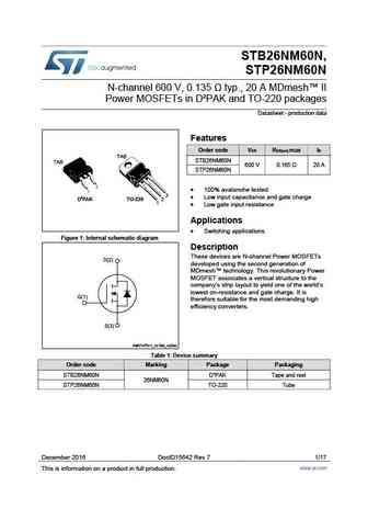
STB26NM60N, STP26NM60N N-channel 600 V, 0.135 typ., 20 A MDmesh II Power MOSFETs in D PAK and TO-220 packages Datasheet - production data Features Order code V R max I DS DS(on) D TAB STB26NM60N TAB 600 V 0.165 20 A STP26NM60N 100% avalanche tested 3 Low input capacitance and gate charge D2PAK TO-220 2 1 Low gate input resistance Application
stb26nm60n stf26nm60n stp26nm60n stw26nm60n.pdf
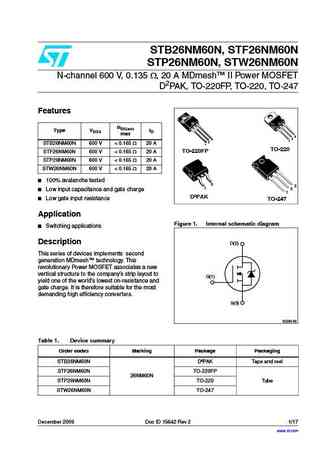
STB26NM60N, STF26NM60N STP26NM60N, STW26NM60N N-channel 600 V, 0.135 , 20 A MDmesh II Power MOSFET D2PAK, TO-220FP, TO-220, TO-247 Features RDS(on) Type VDSS ID max 3 2 3 1 2 STB26NM60N 600 V
stp26nm60n.pdf
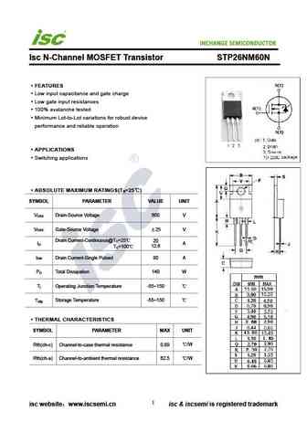
INCHANGE Semiconductor Isc N-Channel MOSFET Transistor STP26NM60N FEATURES Low input capacitance and gate charge Low gate input resistances 100% avalanche tested Minimum Lot-to-Lot variations for robust device performance and reliable operation APPLICATIONS Switching applications ABSOLUTE MAXIMUM RATINGS(T =25 ) a SYMBOL PARAMETER VALUE UNIT V Drain-Source Voltage
Otros transistores... STP24N60M2, STP24N65M2, STP25N10F7, STP25N80K5, STP25NM50N, STP25NM60N, STP260N6F6, STP265N6F6AG, IRF630, STP270N04, IRFR3303PBF, IRFR3410PBF, IRFR3411PBF, IRFR3412PBF, IRFR3418PBF, IRFR3504PBF, IRFR3504ZPBF
🌐 : EN ES РУ

Liste
Recientemente añadidas las descripciónes de los transistores:
MOSFET: AKF30N5P0SX | AKF30N10S | AKF20P45D | CM4407 | CM3407 | CM3400 | SVF11N65F | SVF11N65T | FKBB3105 | EHBA036R1 | CRTT067N10N | AP6NA3R2MT | AP65SA145DDT8 | AP4NAR95CMT-A | AP4024GEMT-HF | AP3P050AH
Popular searches
d313 transistor equivalent | 2sb827 | c5200 datasheet | 2n2614 | 2sa777 replacement | 2sc828 transistor | 2sd357 | 110n8f6 mosfet datasheet