ST1005SRG MOSFET Equivalente. Reemplazo. Hoja de especificaciones. Principales características
Número de Parte: ST1005SRG
Tipo de FET: MOSFET
Polaridad de transistor: P
ESPECIFICACIONES MÁXIMAS
Pdⓘ - Máxima disipación de potencia: 1.25 W
|Vds|ⓘ - Voltaje máximo drenador-fuente: 100 V
|Vgs|ⓘ - Voltaje máximo fuente-puerta: 20 V
|Id|ⓘ - Corriente continua de drenaje: 0.8 A
Tjⓘ - Temperatura máxima de unión: 150 °C
CARACTERÍSTICAS ELÉCTRICAS
trⓘ - Tiempo de subida: 100 nS
Cossⓘ - Capacitancia de salida: 110 pF
RDSonⓘ - Resistencia estado encendido drenaje a fuente: 0.65 Ohm
Encapsulados: SOT-23
Búsqueda de reemplazo de ST1005SRG MOSFET
- Selecciónⓘ de transistores por parámetros
ST1005SRG datasheet
st1005srg.pdf
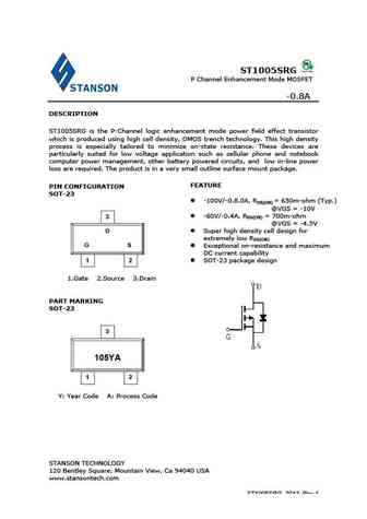
ST1005SRG P Channel Enhancement Mode MOSFET -0.8A DESCRIPTION ST1005SRG is the P-Channel logic enhancement mode power field effect transistor which is produced using high cell density, DMOS trench technology. This high density process is especially tailored to minimize on-state resistance. These devices are particularly suited for low voltage application such as cellular phone an
bst100.pdf
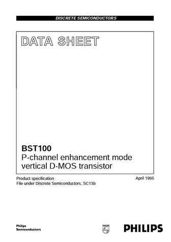
DISCRETE SEMICONDUCTORS DATA SHEET BST100 P-channel enhancement mode vertical D-MOS transistor April 1995 Product specification File under Discrete Semiconductors, SC13b Philips Semiconductors Product specification P-channel enhancement mode vertical BST100 D-MOS transistor DESCRIPTION QUICK REFERENCE DATA P-channel vertical D-MOS transistor Drain-source voltage -VDS max. 60 V T
st1004srg.pdf
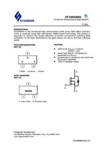
ST1004SRG N Channel Enhancement Mode MOSFET 2.0A DESCRIPTION ST1004SRG is the N-Channel logic enhancement mode power field effect transistor which is produced using high cell density, DMOS trench technology. The process is especially to improve the overall efficiency of DC/DC conventional switching PWM controllers. It has been optimized for low gate charge, low R and fast switchi
st1002.pdf
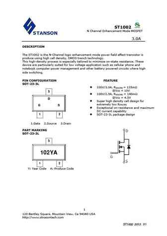
ST1002 N Channel Enhancement Mode MOSFET 3.0A DESCRIPTION The ST1002 is the N-Channel logic enhancement mode power field effect transistor is produce using high cell density, DMOS trench technology. This high-density process is especially tailored to minimize on-state resistance. These device are particularly suited for low voltage application such as cellular phone and notebo
Otros transistores... SRM7N65TC-E1, SS05N70, SS07N70, SSD80N03, SSFM2506L, SSFM2508, ST1002, ST1004SRG, IRF1404, ST10E4, ST12N10D, ST13P10, ST2300, ST2300SRG, ST2301A, ST2302, ST2303SRG
🌐 : EN ES РУ

Liste
Recientemente añadidas las descripciónes de los transistores:
MOSFET: FTF30P35D | FTF25N35DHVT | FTF15N35D | FTE15C35G | FTP02P15G | FTE02P15G | AKF30N5P0SX | AKF30N10S | AKF20P45D | CM4407 | CM3407 | CM3400 | SVF11N65F | SVF11N65T | FKBB3105 | EHBA036R1
Popular searches
irfp4568 | mj15004 | ksc2073 | nte102a | tip31cg | s9015 transistor | irf540z | ss8550 transistor