J211 MOSFET Equivalente. Reemplazo. Hoja de especificaciones. Principales características
Número de Parte: J211
Tipo de FET: JFET
Polaridad de transistor: N
ESPECIFICACIONES MÁXIMAS
Pdⓘ - Máxima
disipación de potencia: 0.4 W
|Vds|ⓘ - Voltaje máximo drenador-fuente: 25 V
|Id|ⓘ - Corriente continua
de drenaje: 0.02 A
Tjⓘ - Temperatura máxima de unión: 150 °C
CARACTERÍSTICAS ELÉCTRICAS
|VGSoff|ⓘ - Voltaje de corte de la puerta: 1 V
Cossⓘ - Capacitancia de salida: 0.8 pF
RDSonⓘ - Resistencia estado encendido drenaje a fuente: 50 Ohm
Encapsulados: TO92
Búsqueda de reemplazo de J211 MOSFET
- Selecciónⓘ de transistores por parámetros
J211 datasheet
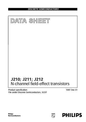
..1. Size:100K philips
j210 j211 j212 1.pdf 

DISCRETE SEMICONDUCTORS DATA SHEET J210; J211; J212 N-channel field-effect transistors Product specification 1997 Dec 01 File under Discrete Semiconductors, SC07 Philips Semiconductors Product specification N-channel field-effect transistors J210; J211; J212 FEATURES PINNING - TO-92 (SOT54) High speed switching PIN SYMBOL DESCRIPTION Interchangeability of drain and source co
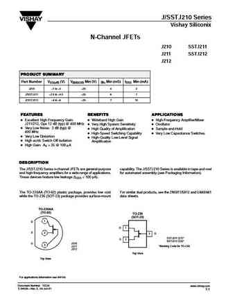
..2. Size:55K vishay
j210 j211 sstj211 j212 sstj212.pdf 

J/SSTJ210 Series Vishay Siliconix N-Channel JFETs J210 SSTJ211 J211 SSTJ212 J212 PRODUCT SUMMARY Part Number VGS(off) (V) V(BR)GSS Min (V) gfs Min (mS) IDSS Min (mA) J210 1 to 3 25 4 2 J/SSTJ211 2.5 to 4.5 25 6 7 J/SSTJ212 4 to 6 25 7 15 FEATURES BENEFITS APPLICATIONS D Excellent High Frequency Gain D Wideband High Gain D High-Frequency Amplifier/Mixer J
0.1. Size:173K motorola
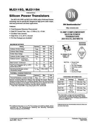
mj21193r.pdf 

Order this document MOTOROLA by MJ21193/D SEMICONDUCTOR TECHNICAL DATA PNP * MJ21193 NPN Silicon Power Transistors * MJ21194 The MJ21193 and MJ21194 utilize Perforated Emitter technology and are *Motorola Preferred Device specifically designed for high power audio output, disk head positioners and linear applications. 16 AMPERE COMPLEMENTARY Total Harmonic Distortion Charac
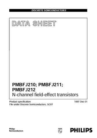
0.2. Size:100K philips
pmbfj210 pmbfj211 pmbfj212 1.pdf 

DISCRETE SEMICONDUCTORS DATA SHEET PMBFJ210; PMBFJ211; PMBFJ212 N-channel field-effect transistors Product specification 1997 Dec 01 File under Discrete Semiconductors, SC07 Philips Semiconductors Product specification N-channel field-effect transistors PMBFJ210; PMBFJ211; PMBFJ212 FEATURES PINNING - SOT23 High speed switching PIN SYMBOL DESCRIPTION Interchangeability of dr
0.4. Size:153K onsemi
mj21194g.pdf 

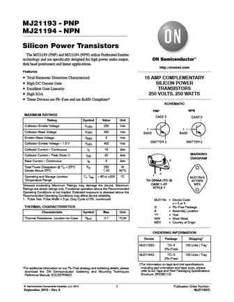
MJ21193, MJ21194 Preferred Device Silicon Power Transistors The MJ21193 (PNP) and MJ21194 (NPN) utilize Perforated Emitter technology and are specifically designed for high power audio output, disk head positioners and linear applications. Features http //onsemi.com Total Harmonic Distortion Characterized High DC Current Gain - hFE = 25 Min @ IC = 8 Adc 16 AMP COMPLEMENTARY
0.5. Size:125K onsemi
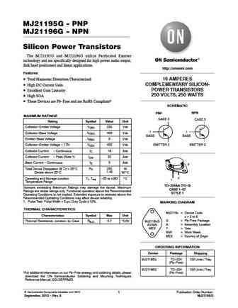
mj21195g mj21196g.pdf 

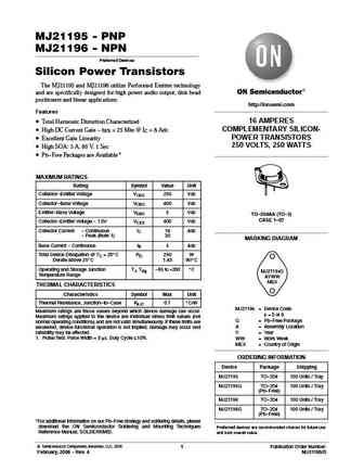
MJ21195G - PNP MJ21196G - NPN Silicon Power Transistors The MJ21195G and MJ21196G utilize Perforated Emitter technology and are specifically designed for high power audio output, disk head positioners and linear applications. http //onsemi.com Features Total Harmonic Distortion Characterized 16 AMPERES COMPLEMENTARY SILICON- High DC Current Gain POWER TRANSISTORS Excelle
0.6. Size:94K onsemi
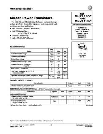
mj21195-96.pdf 

ON Semiconductort PNP * MJ21195 Silicon Power Transistors NPN * MJ21196 The MJ21195 and MJ21196 utilize Perforated Emitter technology and are specifically designed for high power audio output, disk head *ON Semiconductor Preferred Device positioners and linear applications. 16 AMPERE Total Harmonic Distortion Characterized COMPLEMENTARY High DC Current Gain SILICON
0.7. Size:153K onsemi
mj21193g.pdf 

MJ21193, MJ21194 Preferred Device Silicon Power Transistors The MJ21193 (PNP) and MJ21194 (NPN) utilize Perforated Emitter technology and are specifically designed for high power audio output, disk head positioners and linear applications. Features http //onsemi.com Total Harmonic Distortion Characterized High DC Current Gain - hFE = 25 Min @ IC = 8 Adc 16 AMP COMPLEMENTARY
0.8. Size:83K onsemi
mj21196g.pdf 

MJ21195 - PNP MJ21196 - NPN Preferred Devices Silicon Power Transistors The MJ21195 and MJ21196 utilize Perforated Emitter technology and are specifically designed for high power audio output, disk head positioners and linear applications. http //onsemi.com Features Total Harmonic Distortion Characterized 16 AMPERES COMPLEMENTARY SILICON- High DC Current Gain - hFE = 25 Min @
0.9. Size:122K onsemi
mj21193 mj21194.pdf 

MJ21193 - PNP MJ21194 - NPN Silicon Power Transistors The MJ21193 (PNP) and MJ21194 (NPN) utilize Perforated Emitter technology and are specifically designed for high power audio output, disk head positioners and linear applications. http //onsemi.com Features Total Harmonic Distortion Characterized 16 AMP COMPLEMENTARY High DC Current Gain SILICON POWER Excellent Gain Lin
0.10. Size:82K onsemi
mj21195 mj21196.pdf 

MJ21195 - PNP MJ21196 - NPN Preferred Devices Silicon Power Transistors The MJ21195 and MJ21196 utilize Perforated Emitter technology and are specifically designed for high power audio output, disk head positioners and linear applications. http //onsemi.com Features Total Harmonic Distortion Characterized 16 AMPERES COMPLEMENTARY SILICON- High DC Current Gain - hFE = 25 Min @
0.11. Size:83K onsemi
mj21195g.pdf 

MJ21195 - PNP MJ21196 - NPN Preferred Devices Silicon Power Transistors The MJ21195 and MJ21196 utilize Perforated Emitter technology and are specifically designed for high power audio output, disk head positioners and linear applications. http //onsemi.com Features Total Harmonic Distortion Characterized 16 AMPERES COMPLEMENTARY SILICON- High DC Current Gain - hFE = 25 Min @
0.12. Size:1228K kexin
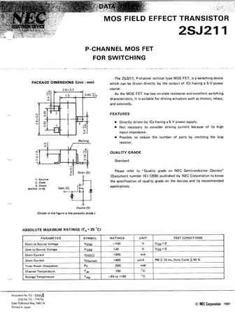
2sj211-3.pdf 

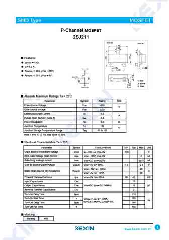
SMD Type MOSFET P-Channel MOSFET 2SJ211 SOT-23-3 Unit mm +0.2 2.9 -0.1 +0.1 0.4 -0.1 3 Features VDS (V) =-100V 1 2 +0.02 ID =-0.2 A +0.1 0.15 -0.02 0.95 -0.1 +0.1 1.9 -0.2 RDS(ON) 20 (VGS =-10V) RDS(ON) 30 (VGS =-4V) 1. Gate 2. Source 3. Drain Absolute Maximum Ratings Ta = 25 Parameter Symbol Rating Unit Drain-Source Voltage
0.13. Size:1220K kexin
2sj211.pdf 

SMD Type MOSFET P-Channel MOSFET 2SJ211 SOT-23 Unit mm +0.1 2.9 -0.1 +0.1 0.4-0.1 3 Features VDS (V) =-100V 1 2 ID =-0.2 A +0.1 +0.05 0.95 -0.1 0.1 -0.01 +0.1 1.9 -0.1 RDS(ON) 20 (VGS =-10V) RDS(ON) 30 (VGS =-4V) 1. Gate 2. Source 3. Drain Absolute Maximum Ratings Ta = 25 Parameter Symbol Rating Unit Drain-Source Voltage VDS
0.14. Size:167K cn sptech
mj21194.pdf 

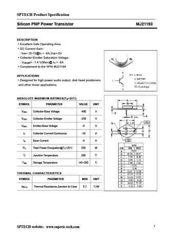
SPTECH Product Specification Silicon NPN Power Transistor MJ21194 DESCRIPTION Excellent Safe Operating Area DC Current Gain- h = 25-75@I = 8A,V = 5V FE C CE Collector-Emitter Saturation Voltage- V )= 1.4 V(Max)@ I = 8A CE(sat C Complement to the PNP MJ21193 APPLICATIONS Designed for high power audio output, disk head positioners and other linear applications. ABSOLUT
0.15. Size:167K cn sptech
mj21193.pdf 

SPTECH Product Specification Silicon PNP Power Transistor MJ21193 DESCRIPTION Excellent Safe Operating Area DC Current Gain- h = 25-75@I = -8A,V =-5V FE C CE Collector-Emitter Saturation Voltage- V )= -1.4 V(Max)@ I = -8A CE(sat C Complement to the NPN MJ21194 APPLICATIONS Designed for high power audio output, disk head positioners and other linear applications. ABSO
0.16. Size:201K inchange semiconductor
mj21194.pdf 

INCHANGE Semiconductor isc Product Specification isc Silicon NPN Power Transistor MJ21194 DESCRIPTION Total Harmonic Distortion Characterized High DC Current Gain High Area of Safe Operation APPLICATIONS Designed for high power audio output, disk head positioners and linear applications. ABSOLUTE MAXIMUM RATINGS(Ta=25 ) SYMBOL PARAMETER VALUE UNIT VCBO Collector-Em
0.17. Size:201K inchange semiconductor
mj21193.pdf 
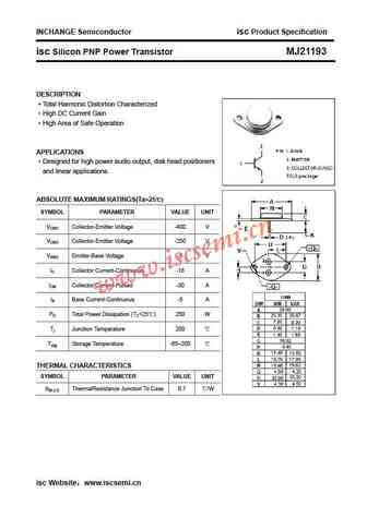
INCHANGE Semiconductor isc Product Specification isc Silicon PNP Power Transistor MJ21193 DESCRIPTION Total Harmonic Distortion Characterized High DC Current Gain High Area of Safe Operation APPLICATIONS Designed for high power audio output, disk head positioners and linear applications. ABSOLUTE MAXIMUM RATINGS(Ta=25 ) SYMBOL PARAMETER VALUE UNIT VCBO Collector-Em
Otros transistores... IXTZ67N10MA, IXTZ67N10MB, J108, J109, J110, J111, J112, J113, IRF3710, J212, JANSR2N7272, JANSR2N7275, JANSR2N7278, JANSR2N7292, JANSR2N7294, JANSR2N7395, JANSR2N7396
