TSM2313CX MOSFET Equivalente. Reemplazo. Hoja de especificaciones. Principales características
Número de Parte: TSM2313CX
Tipo de FET: MOSFET
Polaridad de transistor: P
ESPECIFICACIONES MÁXIMAS
Pdⓘ - Máxima disipación de potencia: 2 W
|Vds|ⓘ - Voltaje máximo drenador-fuente: 20 V
|Vgs|ⓘ - Voltaje máximo fuente-puerta: 12 V
|Id|ⓘ - Corriente continua de drenaje: 3.3 A
Tjⓘ - Temperatura máxima de unión: 150 °C
CARACTERÍSTICAS ELÉCTRICAS
trⓘ - Tiempo de subida: 35 nS
Cossⓘ - Capacitancia de salida: 180 pF
RDSonⓘ - Resistencia estado encendido drenaje a fuente: 0.07 Ohm
Encapsulados: SOT-23
Búsqueda de reemplazo de TSM2313CX MOSFET
- Selecciónⓘ de transistores por parámetros
TSM2313CX datasheet
tsm2311cx.pdf
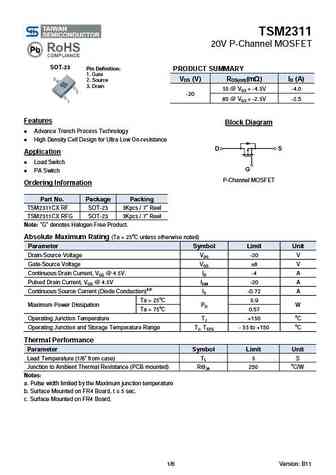
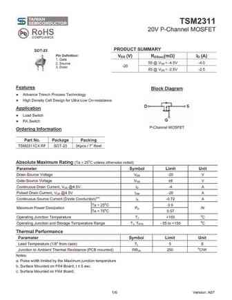
TSM2311 20V P-Channel MOSFET SOT-23 Pin Definition PRODUCT SUMMARY 1. Gate VDS (V) RDS(on)(m ) ID (A) 2. Source 3. Drain 55 @ VGS = -4.5V -4.0 -20 85 @ VGS = -2.5V -2.5 Features Block Diagram Advance Trench Process Technology High Density Cell Design for Ultra Low On-resistance Application Load Switch PA Switch P-Channel MOSFET Orderi
tsm2314cx.pdf
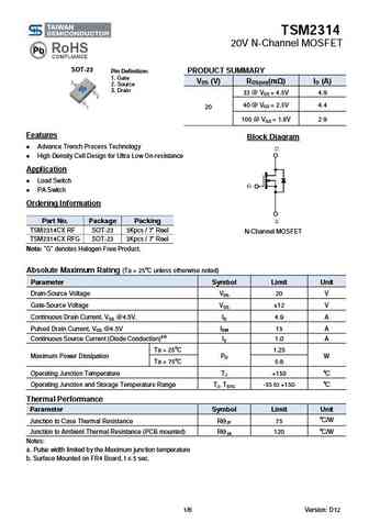
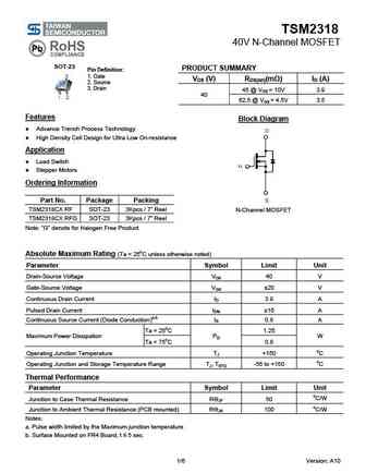
TSM2314 20V N-Channel MOSFET SOT-23 PRODUCT SUMMARY Pin Definition 1. Gate VDS (V) RDS(on)(m ) ID (A) 2. Source 3. Drain 33 @ VGS = 4.5V 4.9 40 @ VGS = 2.5V 4.4 20 100 @ VGS = 1.8V 2.9 Features Block Diagram Advance Trench Process Technology High Density Cell Design for Ultra Low On-resistance Application Load Switch PA Switch Orderin

Otros transistores... TSM2303CX, TSM2305CX, TSM2306CX, TSM2307CX, TSM2308CX, TSM2310CX, TSM2311CX, TSM2312CX, AO4407A, TSM2314CX, TSM2318CX, TSM2323CX, TSM2328CX, TSM23N50CN, TSM25N03CP, TSM2611EDCX6, TSM2N60CH
History: BRCS050N04RA | BL13N25-A
🌐 : EN ES РУ

Liste
Recientemente añadidas las descripciónes de los transistores:
MOSFET: AUP060N055 | AUP056N10 | AUP056N08BGL | AUP052N085 | AUP045N12 | AUP039N10 | AUP034N10 | AUP034N06 | AUP033N08BG | AUP026N085 | AUN084N10 | AUN065N10 | AUN063N10 | AUN062N08BG | AUN060N08AG | AUN053N10
Popular searches
2sc984 | 2sa872 | 2sc1222 | 2sc2581 | c1061 transistor | 2sc1451 | c3199 transistor | 2n2712 datasheet