TSM3401CX MOSFET Equivalente. Reemplazo. Hoja de especificaciones. Principales características
Número de Parte: TSM3401CX
Tipo de FET: MOSFET
Polaridad de transistor: P
ESPECIFICACIONES MÁXIMAS
Pdⓘ - Máxima disipación de potencia: 1.25 W
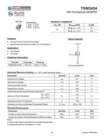
|Vds|ⓘ - Voltaje máximo drenador-fuente: 30 V
|Vgs|ⓘ - Voltaje máximo fuente-puerta: 20 V
|Id|ⓘ - Corriente continua de drenaje: 3 A
Tjⓘ - Temperatura máxima de unión: 150 °C
CARACTERÍSTICAS ELÉCTRICAS
trⓘ - Tiempo de subida: 2.33 nS
Cossⓘ - Capacitancia de salida: 90.96 pF
RDSonⓘ - Resistencia estado encendido drenaje a fuente: 0.06 Ohm
Encapsulados: SOT-23
Búsqueda de reemplazo de TSM3401CX MOSFET
- Selecciónⓘ de transistores por parámetros
TSM3401CX datasheet
tsm3401cx.pdf
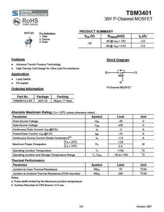
TSM3401 30V P-Channel MOSFET PRODUCT SUMMARY SOT-23 Pin Definition 1. Gate VDS (V) RDS(on)(m ) ID (A) 2. Source 60 @ VGS = 10V -3.0 3. Drain -30 90 @ VGS = 4.5V -2.0 Features Block Diagram Advance Trench Process Technology High Density Cell Design for Ultra Low On-resistance Application Load Switch PA Switch P-Channel MOSFET Ordering Info
tsm3400cx.pdf
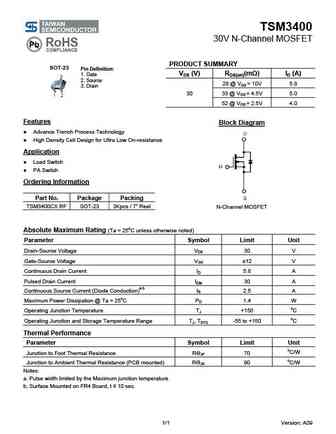
TSM3400 30V N-Channel MOSFET PRODUCT SUMMARY SOT-23 Pin Definition VDS (V) RDS(on)(m ) ID (A) 1. Gate 2. Source 28 @ VGS = 10V 5.8 3. Drain 30 33 @ VGS = 4.5V 5.0 52 @ VGS = 2.5V 4.0 Features Block Diagram Advance Trench Process Technology High Density Cell Design for Ultra Low On-resistance Application Load Switch PA Switch Ordering Infor
tsm3404cx.pdf
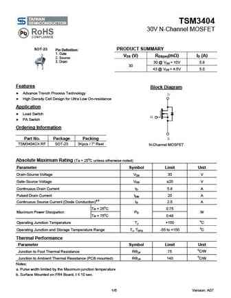
TSM3404 30V N-Channel MOSFET SOT-23 PRODUCT SUMMARY Pin Definition 1. Gate VDS (V) RDS(on)(m ) ID (A) 2. Source 3. Drain 30 @ VGS = 10V 5.8 30 43 @ VGS = 4.5V 5.0 Features Block Diagram Advance Trench Process Technology High Density Cell Design for Ultra Low On-resistance Application Load Switch PA Switch Ordering Information Part No. Pac
tsm3424cx6.pdf
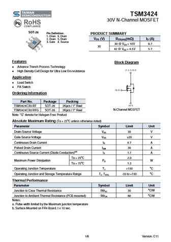
TSM3424 30V N-Channel MOSFET SOT-26 Pin Definition PRODUCT SUMMARY 1. Drain 6. Drain 2. Drain 5, Drain VDS (V) RDS(on)(m ) ID (A) 3. Gate 4. Source 30 @ VGS = 10V 6.7 30 42 @ VGS = 4.5V 5.7 Features Block Diagram Advance Trench Process Technology High Density Cell Design for Ultra Low On-resistance Application Load Switch PA Switch Orderin
Otros transistores... TSM2N70CP, TSM2N70CZ, TSM2NB60CH, TSM2NB60CI, TSM2NB60CP, TSM2NB60CZ, TSM301K12CQ, TSM3400CX, AON6414A, TSM3404CX, TSM3424CX6, TSM3433CX6, TSM3441CX6, TSM3442CX6, TSM3443CX6, TSM3446CX6, TSM3454CX6
History: IRLI2505
🌐 : EN ES РУ

Liste
Recientemente añadidas las descripciónes de los transistores:
MOSFET: AUP060N055 | AUP056N10 | AUP056N08BGL | AUP052N085 | AUP045N12 | AUP039N10 | AUP034N10 | AUP034N06 | AUP033N08BG | AUP026N085 | AUN084N10 | AUN065N10 | AUN063N10 | AUN062N08BG | AUN060N08AG | AUN053N10
Popular searches
oc71 | njw0302g | 2n3904 transistor equivalent | 2sc2312 | bu406 datasheet | irfb7437 | tip32a | p75nf75 mosfet equivalent