K2611S MOSFET Equivalente. Reemplazo. Hoja de especificaciones. Principales características
Número de Parte: K2611S
Tipo de FET: MOSFET
Polaridad de transistor: N
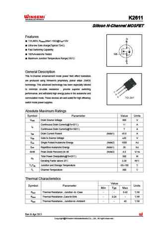
ESPECIFICACIONES MÁXIMAS
Pdⓘ - Máxima disipación de potencia: 276 W
|Vds|ⓘ - Voltaje máximo drenador-fuente: 900 V
|Vgs|ⓘ - Voltaje máximo fuente-puerta: 30 V
|Id|ⓘ - Corriente continua de drenaje: 9 A
Tjⓘ - Temperatura máxima de unión: 150 °C
CARACTERÍSTICAS ELÉCTRICAS
trⓘ - Tiempo de subida: 25 nS
Cossⓘ - Capacitancia de salida: 190 pF
RDSonⓘ - Resistencia estado encendido drenaje a fuente: 1.35 Ohm
Encapsulados: TO-247
Búsqueda de reemplazo de K2611S MOSFET
- Selecciónⓘ de transistores por parámetros
K2611S datasheet
k2611s.pdf
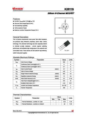
K2611S K2611S K2611S K2611S Silicon N-Channel MOSFET Silicon N-Channel MOSFET Silicon N-Channel MOSFET Silicon N-Channel MOSFET Features 9A,900V, R (Max1.35 )@V =10V DS(on) GS Ultra-low Gate charge(Typical 58nC) Fast Switching Capability 100%Avalanche Tested Maximum Junction Temperature Range(150 ) General Description This N-Channel enhancement mode power
k2611sb.pdf
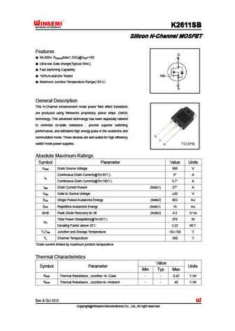
K2611SB K2611SB K2611SB K2611SB Silicon N-Channel MOSFET Silicon N-Channel MOSFET Silicon N-Channel MOSFET Silicon N-Channel MOSFET Features 9A,900V, R (Max1.35 )@V =10V DS(on) GS Ultra-low Gate charge(Typical 58nC) Fast Switching Capability 100%Avalanche Tested Maximum Junction Temperature Range(150 ) General Description This N-Channel enhancement mode p
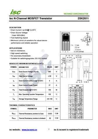
2sk2611.pdf
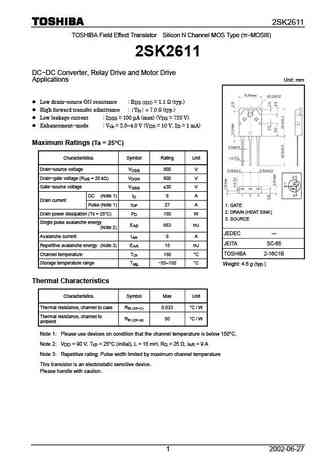
2SK2611 TOSHIBA Field Effect Transistor Silicon N Channel MOS Type ( -MOSIII) 2SK2611 DC-DC Converter, Relay Drive and Motor Drive Applications Unit mm Low drain-source ON resistance RDS = 1.1 (typ.) (ON) High forward transfer admittance Y 7.0 S (typ.) fs = Low leakage current I = 100 A (max) (V = 720 V) DSS DS Enhancement-mode Vth = 2.0 4.0 V (V =
k2611b.pdf
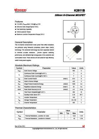
K2611B K2611B K2611B K2611B Silicon N-Channel MOSFET Silicon N-Channel MOSFET Silicon N-Channel MOSFET Silicon N-Channel MOSFET Features 11A,900V, R (Max1.10 )@V =10V DS(on) GS Ultra-low Gate charge(Typical 72nC) Fast Switching Capability 100%Avalanche Tested Maximum Junction Temperature Range(150 ) General Description This N-Channel enhancement mode powe
Otros transistores... CSD87351Q5D, CSD87352Q5D, CSD87353Q5D, CSD87501L, CSD88539ND, CSD9024, K2611, K2611B, 18N50, K2611SB, K2698, K2698B, K2837, K2837B, KDB15N50, KDB2532, KDB2552
🌐 : EN ES РУ

Liste
Recientemente añadidas las descripciónes de los transistores:
MOSFET: FTF30P35D | FTF25N35DHVT | FTF15N35D | FTE15C35G | FTP02P15G | FTE02P15G | AKF30N5P0SX | AKF30N10S | AKF20P45D | CM4407 | CM3407 | CM3400 | SVF11N65F | SVF11N65T | FKBB3105 | EHBA036R1
Popular searches
2n3035 transistor | 2sb649a | 2sd188 | k b778 transistor | 2n5133 datasheet | 2sa726 transistor | 7506 mosfet | irlr8726 datasheet