KI2306 Datasheet. Equivalente. Reemplazo. Hoja de especificaciones. Principales características
Número de Parte: KI2306 📄📄
Tipo de FET: MOSFET
Polaridad de transistor: N
ESPECIFICACIONES MÁXIMAS
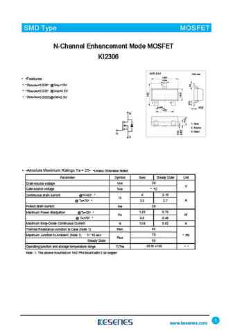
Pdⓘ - Máxima disipación de potencia: 0.75 W
|Vds|ⓘ - Voltaje máximo drenador-fuente: 30 V
|Vgs|ⓘ - Voltaje máximo fuente-puerta: 12 V
|Id|ⓘ - Corriente continua de drenaje: 3.16 A
Tjⓘ - Temperatura máxima de unión: 150 °C
CARACTERÍSTICAS ELÉCTRICAS
trⓘ - Tiempo de subida: 14 nS
Cossⓘ - Capacitancia de salida: 64 pF
RDSonⓘ - Resistencia estado encendido drenaje a fuente: 0.03 Ohm
Encapsulados: SOT-23
📄📄 Copiar
Búsqueda de reemplazo de KI2306 MOSFET
- Selecciónⓘ de transistores por parámetros
KI2306 datasheet
..1. Size:1581K kexin
si2306 ki2306.pdf 
SMD Type MOSFET IC N-Channel 30-V (D-S) MOSFET SI2306 (KI2306) SOT-23-3 Unit mm +0.2 2.9 -0.1 +0.1 0.4-0.1 Features 3 VDS (V) = 30V RDS(ON) 57m (VGS =-10V) RDS(ON) 94 m (VGS =-4.5V) 1 2 +0.02 +0.1 D 0.15 -0.02 0.95 -0.1 +0.1 1.9 -0.2 G 1. Gate 2. Source S 3. Drain Absolute Maximum Ratings Ta = 25 Parameter Symbol Rating Unit Drain-S
..2. Size:1075K kesenes
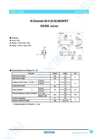
ki2306.pdf
SMD Type IC SMD Type MOSFET N-Channel Enhancement Mode MOSFET KI2306 SOT-23-3 Unit mm +0.2 2.9-0.2 Features 0.4+0.1 -0.05 3 @VGS=10V RDS(ON)=0.030 RDS(ON)=0.035 @VGS=4.5V DS(ON) GS R =0.052 @V =2.5V 12 0.95+0.1 -0.1 0.1+0.05 -0.01 1.9+0.2 -0.2 D 1.Base 1. Gate 2.Emitter 2. Source 3. Drain 3.collector G S Absolute Maximum Ratings
0.1. Size:47K kexin
ki2306ds.pdf
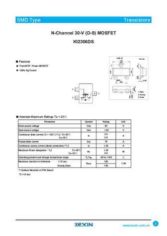
SMD Type IC SMD Type Transistors N-Channel 30-V (D-S) MOSFET KI2306DS SOT-23 Unit mm +0.1 2.9-0.1 Features +0.1 0.4-0.1 3 TrenchFET Power MOSFET 100% Rg Tested 12 +0.1 +0.05 0.95-0.1 0.1-0.01 +0.1 1.9-0.1 1.Base 1. Gate 2.Emitter 2. Source 3. Drain 3.collector Absolute Maximum Ratings Ta = 25 Parameter Symbol Rating Unit Drain-source voltage VDS 30 V Gate-source vol
9.2. Size:321K tysemi
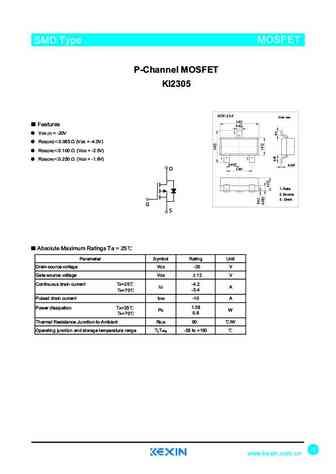
ki2305.pdf
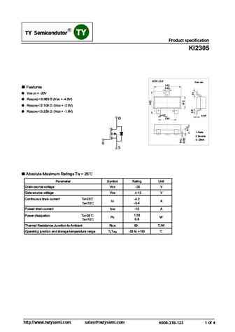
SMD Type MOSFET Product specification KI2305 SOT-23-3 Unit mm 2.9+0.2 -0.2 Features 0.4+0.1 -0.05 3 VDS (V) = -20V RDS(ON) 0.065 (VGS = -4.5V) RDS(ON) 0.100 (VGS = -2.5V) 12 RDS(ON) 0.250 (VGS = -1.8V) +0.1 0.95-0.1 0.1+0.05 -0.01 +0.2 1.9-0.2 D 1. Gate 2. Source 3. Drain G S Absolute Maximum Ratings Ta = 25 Parameter Sym
9.3. Size:921K tysemi
ki2303ds.pdf
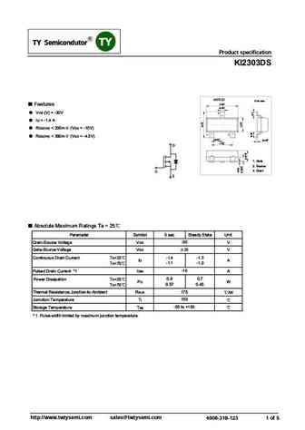
SMD Type IC SMD Type MOSFE SMD Type MOSFET SMD Type MOSFET SMD Type MOSFET SMD Type IC Product specification KI2303 DS SOT-23 Unit mm +0.1 2.9-0.1 Features +0.1 0.4-0.1 VDS (V) = -30V 3 ID = -1.4 A RDS(ON)
9.4. Size:197K tysemi
ki2307ds.pdf
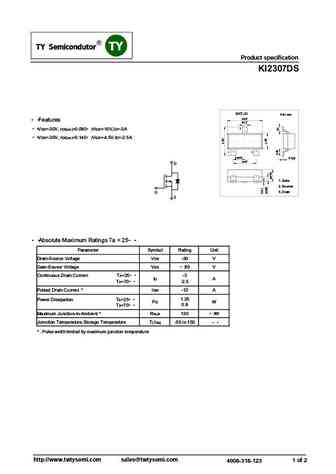
SMD Type IC SMD Type IC SMD Type IC SMD Type MOSFET SMD Type MOSFET SMD Type MOSFE SMD Type MOSFET SMD Type MOSFET SMD Type MOSFET SMD Type IC Product specification KI2307DS SOT-23 Unit mm +0.1 2.9-0.1 Features +0.1 0.4-0.1 3 VDS=-30V, rDS(on)=0.080 ,VGS=-10V,ID=-3A VDS=-30V, rDS(on)=0.140 ,VGS=-4.5V,ID=-2.5A 1 2 +0.1 +0.05 0.95-0.1 0.1
9.5. Size:351K tysemi
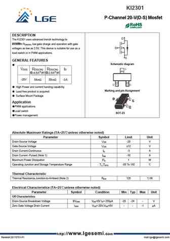
ki2301ds.pdf
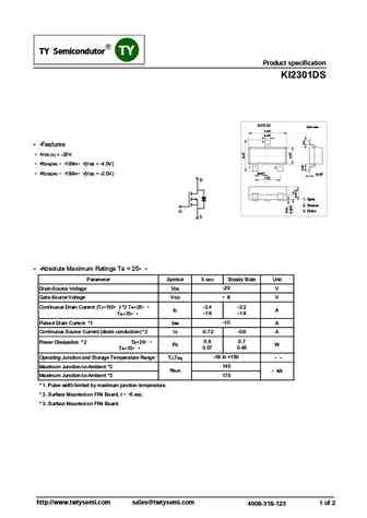
SMD Type IC SMD Type MOSFE SMD Type MOSFET SMD Type MOSFET SMD Type MOSFET Product specification KI2301 DS SOT-23 Unit mm +0.1 2.9-0.1 +0.1 0.4-0.1 3 Features VDS (V) = -20V RDS(ON) 100m (VGS = -4.5V) 1 2 +0.1 +0.05 RDS(ON) 150m (VGS = -2.5V) 0.95-0.1 0.1-0.01 +0.1 1.9-0.1 D 1.Base 1.Base 1. Gate 2.Emitter 2.Emitter 2. Source 3.
9.6. Size:148K tysemi
ki2302ds.pdf
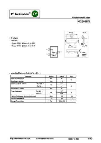
SMD Type SMD Type IC Product specification KI2302DS SOT-23 Unit mm +0.1 2.9-0.1 +0.1 0.4-0.1 3 Features VDS=20V RDS(on)= 0.085 @VGS=4.5V ,ID=3.6A 1 2 +0.1 +0.05 0.95-0.1 0.1-0.01 RDS(on)= 0.115 @VGS=2.5V ,ID= 3.1A +0.1 1.9-0.1 G 1 3 D 1.Base 1. Gate S 2 2.Emitter 2. Source 3. Drain 3.collector Absolute Maximum Ratings Ta = 25 Parameter
9.7. Size:51K kexin
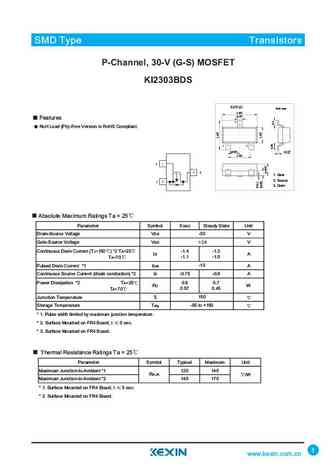
ki2307bds.pdf
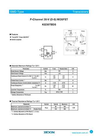
SMD Type IC SMD Type Transistors P-Channel 30-V (D-S) MOSFET KI2307BDS SOT-23 Unit mm +0.1 2.9-0.1 +0.1 0.4-0.1 Features 3 TrenchFET Power MOSFET RoHS Compliant 12 +0.1 +0.05 0.95-0.1 0.1-0.01 +0.1 1.9-0.1 1.Base 1. Gate 2.Emitter 2. Source 3. Drain 3.collector Absolute Maximum Ratings Ta = 25 Parameter Symbol 5 sec Steady State Unit Drain-Source Voltage VDS -30 V
9.8. Size:1560K kexin
si2302 ki2302.pdf
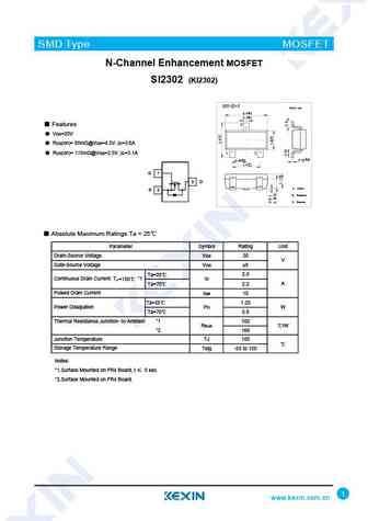
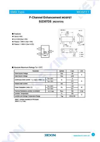
SMD Type MOSFET N-Channel Enhancement MOSFET SI2302 (KI2302) SOT-23-3 Unit mm +0.2 2.9 -0.1 +0.1 0.4-0.1 3 Features VDS=20V RDS(on)= 85m @VGS=4.5V ,ID=3.6A RDS(on)= 115m @VGS=2.5V ,ID=3.1A 1 2 +0.02 +0.1 0.15 -0.02 0.95 -0.1 +0.1 1.9 -0.2 G 1 3 D 1. Gate S 2 2. Source 3. Drain Absolute Maximum Ratings Ta = 25 Parameter Symbol Rating Unit Dr
9.9. Size:1036K kexin
ki2305ds.pdf
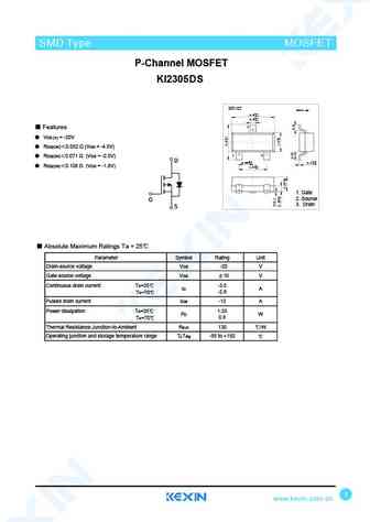
SMD Type MOSFET SMD Type P-Channel MOSFET KI2305DS SOT-23 Unit mm 2.9+0.1 -0.1 +0.1 0.4-0.1 3 Features VDS (V) = -20V RDS(ON) 0.052 (VGS = -4.5V) 1 2 RDS(ON) 0.071 (VGS = -2.5V) D +0.1 +0.05 0.95 -0.1 0.1 -0.01 RDS(ON) 0.108 (VGS = -1.8V) +0.1 1.9 -0.1 1. Gate 2. Source G 3. Drain S Absolute Maximum Ratings Ta = 25 Paramet
9.10. Size:49K kexin
ki2301bds.pdf
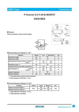
SMD Type Transistors P-Channel 2.5-V (G-S) MOSFET KI2301BDS SOT-23 Unit mm +0.1 2.9-0.1 +0.1 0.4-0.1 3 Features 12 RoH Lead (Pb)-Free Version is RoHS Compliant. +0.1 +0.05 0.95-0.1 0.1-0.01 +0.1 1.9-0.1 1.Base 1. Gate 2.Emitter 2. Source 3. Drain 3.collector Absolute Maximum Ratings Ta = 25 Parameter Symbol 5 sec Steady State Unit Drain-Source Voltage VDS -20 V Gate-
9.11. Size:48K kexin
ki2300.pdf
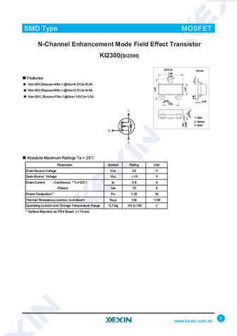
SMD Type IC SMD Type MOSFET N-Channel Enhancement Mode Field Effect Transistor KI2300(SI2300) SOT-23 Unit mm +0.1 2.9-0.1 +0.1 0.4-0.1 Features 3 VDS=20V,RDS(ON)=40m @VGS=4.5V,ID=5.0A VDS=20V,RDS(ON)=60m @VGS=2.5V,ID=4.0A VDS=20V,,RDS(ON)=75m @VGS=1.8V,ID=1.0A 12 +0.1 +0.05 0.95-0.1 0.1-0.01 +0.1 1.9-0.1 1.Base 1. Gate 2.Emitter 2. Source 3. Drain 3.collector Absolute
9.12. Size:206K kexin
si2300 ki2300.pdf
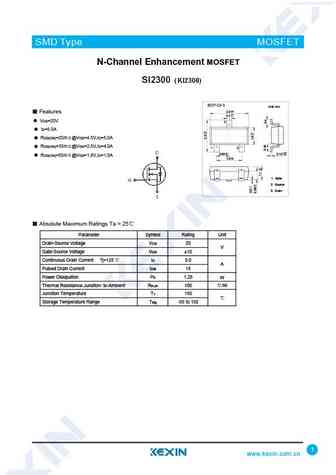
SMD Type IC SMD Type MOSFET N-Channel Enhancement MOSFET SI2300 (KI2300) SOT-23-3 Unit mm +0.2 2.9 -0.1 Features +0.1 0.4 -0.1 VDS=20V 3 ID=5.0A RDS(ON)=25m @VGS=4.5V,ID=5.0A RDS(ON)=35m @VGS=2.5V,ID=4.0A 1 2 +0.02 +0.1 0.15 -0.02 0.95 -0.1 RDS(ON)=55m @VGS=1.8V,ID=1.0A +0.1 1.9 -0.2 1. Gate 2. Source 3. Drain Absolute Maximum Ratings Ta = 25 Parameter Symbol Rating
9.13. Size:307K kexin
ki2305.pdf
SMD Type MOSFET P-Channel MOSFET KI2305 SOT-23-3 Unit mm 2.9+0.2 -0.2 Features 0.4+0.1 -0.05 3 VDS (V) = -20V RDS(ON) 0.065 (VGS = -4.5V) RDS(ON) 0.100 (VGS = -2.5V) 12 RDS(ON) 0.250 (VGS = -1.8V) +0.1 0.95-0.1 0.1+0.05 -0.01 +0.2 1.9-0.2 D 1. Gate 2. Source 3. Drain G S Absolute Maximum Ratings Ta = 25 Parameter Symbol R
9.14. Size:52K kexin
ki2303bds.pdf
SMD Type Transistors P-Channel, 30-V (G-S) MOSFET KI2303BDS SOT-23 Unit mm +0.1 2.9-0.1 +0.1 0.4-0.1 Features 3 RoH Lead (Pb)-Free Version is RoHS Compliant. 12 +0.1 +0.05 0.95-0.1 0.1-0.01 +0.1 1.9-0.1 1.Base 1. Gate 2.Emitter 2. Source 3. Drain 3.collector Absolute Maximum Ratings Ta = 25 Parameter Symbol 5 sec Steady State Unit Drain-Source Voltage VDS -30 V Gate-
9.15. Size:1589K kexin
si2303 ki2303.pdf
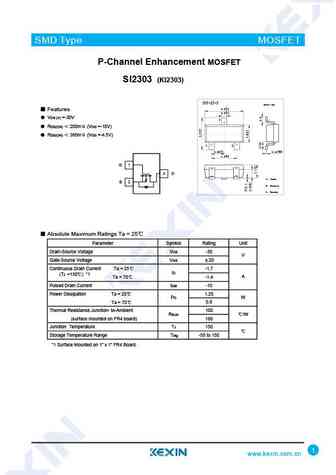
SMD Type MOSFET P-Channel Enhancement MOSFET SI2303 (KI2303) SOT-23-3 Unit mm +0.2 2.9-0.1 Features +0.1 0.4 -0.1 VDS (V) =-30V 3 RDS(ON) 200m (VGS =-10V) RDS(ON) 380m (VGS =-4.5V) 1 2 +0.02 +0.1 0.15 -0.02 0.95 -0.1 +0.1 1.9 -0.2 G 1 3 D 1. Gate S 2 2. Source 3. Drain Absolute Maximum Ratings Ta = 25 Parameter Symbol Rating Un
9.16. Size:322K kexin
ki2301t.pdf
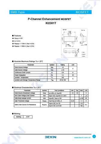
SMD Type MOSFET P-Channel Enhancement MOSFET KI2301T SOT-23 Unit mm +0.1 2.9-0.1 +0.1 0.4 -0.1 3 Features VDS (V) =-12V ID =-2.8 A 1 2 RDS(ON) 115m (VGS =-4.5V) +0.1 +0.05 0.95-0.1 0.1 -0.01 1.9+0.1 -0.1 RDS(ON) 160m (VGS =-2.5V) 1.Gate 2.Source 3.Drain Absolute Maximum Ratings Ta = 25 Parameter Symbol Rating Unit Drain-Sou
9.17. Size:1329K kexin
si2308ds ki2308ds.pdf
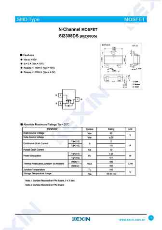
SMD Type MOSFET N-Channel MOSFET SI2308DS (KI2308DS) SOT-23-3 Unit mm +0.2 2.9 -0.1 +0.1 0.4 -0.1 3 Features VDS (V) = 60V ID = 2 A (VGS = 10V) 1 2 +0.02 RDS(ON) 160m (VGS = 10V) +0.1 0.15 -0.02 0.95 -0.1 +0.1 1.9 -0.2 RDS(ON) 220m (VGS = 4.5V) 1. Gate 2. Source 3. Drain G 1 3 D S 2 Absolute Maximum Ratings Ta = 25 Paramete
9.18. Size:185K kexin
si2301 ki2301.pdf
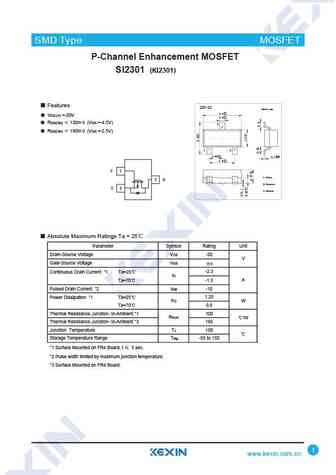
SMD Type MOSFET P-Channel Enhancement MOSFET SI2301 (KI2301) Features VDS (V) =-20V RDS(ON) 130m (VGS =-4.5V) 3 RDS(ON) 190m (VGS =-2.5V) 12 Absolute Maximum Ratings Ta = 25 Parameter Symbol Rating Unit Drain-Source Voltage VDS -20
9.19. Size:50K kexin
ki2309ds.pdf
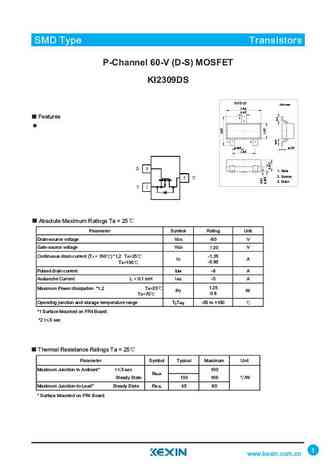
SMD Type Transistors P-Channel 60-V (D-S) MOSFET KI2309DS SOT-23 Unit mm +0.1 2.9-0.1 +0.1 0.4-0.1 Features 3 12 +0.1 +0.05 0.95-0.1 0.1-0.01 +0.1 1.9-0.1 1.Base 1. Gate 2.Emitter 2. Source 3. Drain 3.collector Absolute Maximum Ratings Ta = 25 Parameter Symbol Rating Unit Drain-source voltage VDS -60 V Gate-source voltage VGS 20 V Continuous drain current (TJ = 150 )
9.21. Size:206K kexin
ki2302ds.pdf
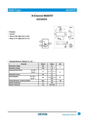
SMD Type Diodes SMD Type MOSFET SMD Type MOSFET N-Channel MOSFET KI2302DS SOT-23 Unit mm +0.1 2.9-0.1 +0.1 0.4-0.1 3 Features VDS=20V RDS(on)= 0.085 @VGS=4.5V ,ID=3.6A 1 2 +0.1 +0.05 0.95-0.1 0.1-0.01 RDS(on)= 0.115 @VGS=2.5V ,ID= 3.1A +0.1 1.9-0.1 G 1 3 D 1.Base 1. Gate S 2 2.Emitter 2. Source 3. Drain 3.collector Absolute Maximum Ratings
9.22. Size:49K kexin
ki2304ds.pdf
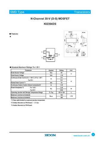
SMD Type Transistors N-Channel 30-V (D-S) MOSFET KI2304DS SOT-23 Unit mm +0.1 2.9-0.1 Features +0.1 0.4-0.1 3 12 +0.1 +0.05 0.95-0.1 0.1-0.01 +0.1 1.9-0.1 1.Base 1. Gate 2.Emitter 2. Source 3. Drain 3.collector Absolute Maximum Ratings Ta = 25 Parameter Symbol Rating Unit Drain-Source Voltage VDS 30 V Gate-Source Voltage VGS 20 Continuous Drain Current (TJ = 150 ) *
9.23. Size:1555K kexin
si2304ds ki2304ds.pdf
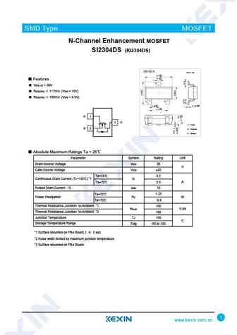
SMD Type MOSFET N-Channel Enhancement MOSFET SI2304DS (KI2304DS) SOT-23-3 Unit mm +0.2 2.9 -0.1 +0.1 0.4-0.1 Features 3 VDS (V) = 30V RDS(ON) 117m (VGS = 10V) RDS(ON) 190m (VGS = 4.5V) 1 2 +0.02 +0.1 0.15 -0.02 0.95 -0.1 +0.1 1.9 -0.2 G 1 3 D 1. Gate S 2 2. Source 3. Drain Absolute Maximum Ratings Ta = 25 Parameter Symbol Ratin
Otros transistores... KI2300, KI2301BDS, KI2301DS, KI2302DS, KI2303BDS, KI2303DS, KI2304DS, KI2305, TK10A60D, KI2306DS, KI2307BDS, KI2307DS, KI2309DS, KI2311DS, KI2312DS, KI2314EDS, KI2315BDS