NVD4813NH Datasheet. Equivalente. Reemplazo. Hoja de especificaciones. Principales características
Número de Parte: NVD4813NH
Tipo de FET: MOSFET
Polaridad de transistor: N
ESPECIFICACIONES MÁXIMAS
Pdⓘ - Máxima
disipación de potencia: 35.3 W
|Vds|ⓘ - Voltaje máximo drenador-fuente: 30 V
|Vgs|ⓘ - Voltaje máximo fuente-puerta: 20 V
|Id|ⓘ - Corriente continua
de drenaje: 40 A
Tjⓘ - Temperatura máxima de unión: 175 °C
CARACTERÍSTICAS ELÉCTRICAS
trⓘ - Tiempo
de subida: 19.5 nS
Cossⓘ - Capacitancia de salida: 201 pF
RDSonⓘ - Resistencia estado encendido drenaje a fuente: 0.013 Ohm
Encapsulados: DPAK
Búsqueda de reemplazo de NVD4813NH MOSFET
- Selecciónⓘ de transistores por parámetros
NVD4813NH datasheet
..2. Size:108K onsemi
nvd4813nh.pdf 
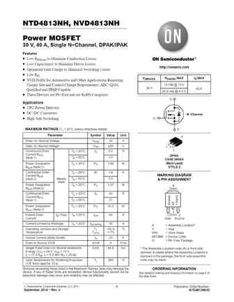
NTD4813NH, NVD4813NH Power MOSFET 30 V, 40 A, Single N-Channel, DPAK/IPAK Features Low RDS(on) to Minimize Conduction Losses Low Capacitance to Minimize Driver Losses http //onsemi.com Optimized Gate Charge to Minimize Switching Losses Low RG V(BR)DSS RDS(ON) MAX ID MAX NVD Prefix for Automotive and Other Applications Requiring 13 mW @ 10 V Unique Site and Contro
8.1. Size:148K onsemi
ntd4810n-1g nvd4810n.pdf
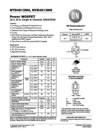
NTD4810N, NVD4810N Power MOSFET 30 V, 54 A, Single N-Channel, DPAK/IPAK Features Low RDS(on) to Minimize Conduction Losses Low Capacitance to Minimize Driver Losses http //onsemi.com Optimized Gate Charge to Minimize Switching Losses AEC-Q101 Qualified and PPAP Capable - NVD4810N V(BR)DSS RDS(on) MAX ID MAX These Devices are Pb-Free and are RoHS Compliant 10 mW @
9.1. Size:114K onsemi
nvd4806n.pdf
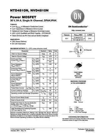
NTD4806N, NVD4806N Power MOSFET 30 V, 76 A, Single N-Channel, DPAK/IPAK Features Low RDS(on) to Minimize Conduction Losses Low Capacitance to Minimize Driver Losses http //onsemi.com Optimized Gate Charge to Minimize Switching Losses AEC-Q101 Qualified and PPAP Capable - NVD4806N V(BR)DSS RDS(on) MAX ID MAX These Devices are Pb-Free and are RoHS Compliant 6.0 mW @
9.2. Size:113K onsemi
nvd4809n.pdf
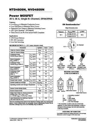
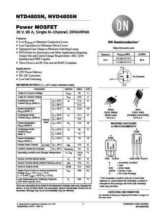
NTD4809N, NVD4809N Power MOSFET 30 V, 58 A, Single N-Channel, DPAK/IPAK Features Low RDS(on) to Minimize Conduction Losses Low Capacitance to Minimize Driver Losses http //onsemi.com Optimized Gate Charge to Minimize Switching Losses AEC Q101 Qualified - NVD4809N V(BR)DSS RDS(on) MAX ID MAX These Devices are Pb-Free and are RoHS Compliant 9.0 mW @ 10 V 30 V 58 A
9.3. Size:116K onsemi
ntd4805n nvd4805n.pdf

NTD4805N, NVD4805N Power MOSFET 30 V, 88 A, Single N-Channel, DPAK/IPAK Features Low RDS(on) to Minimize Conduction Losses Low Capacitance to Minimize Driver Losses http //onsemi.com Optimized Gate Charge to Minimize Switching Losses NVD Prefix for Automotive and Other Applications Requiring V(BR)DSS RDS(on) MAX ID MAX Unique Site and Control Change Requirements; AEC-Q
9.4. Size:117K onsemi
ntd4809n nvd4809n.pdf

NTD4809N, NVD4809N Power MOSFET 30 V, 58 A, Single N-Channel, DPAK/IPAK Features Low RDS(on) to Minimize Conduction Losses Low Capacitance to Minimize Driver Losses http //onsemi.com Optimized Gate Charge to Minimize Switching Losses AEC Q101 Qualified - NVD4809N V(BR)DSS RDS(on) MAX ID MAX These Devices are Pb-Free and are RoHS Compliant 9.0 mW @ 10 V 30 V 58 A
9.5. Size:82K onsemi
nvd4804n.pdf
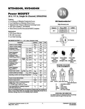
NTD4804N, NVD4804N Power MOSFET 30 V, 117 A, Single N-Channel, DPAK/IPAK Features Low RDS(on) to Minimize Conduction Losses Low Capacitance to Minimize Driver Losses http //onsemi.com Optimized Gate Charge to Minimize Switching Losses AEC Q101 Qualified - NVD4804N V(BR)DSS RDS(on) MAX ID MAX These Devices are Pb-Free and are RoHS Compliant 4.0 mW @ 10 V 30 V 117
9.6. Size:113K onsemi
nvd4805n.pdf
NTD4805N, NVD4805N Power MOSFET 30 V, 88 A, Single N-Channel, DPAK/IPAK Features Low RDS(on) to Minimize Conduction Losses Low Capacitance to Minimize Driver Losses http //onsemi.com Optimized Gate Charge to Minimize Switching Losses NVD Prefix for Automotive and Other Applications Requiring V(BR)DSS RDS(on) MAX ID MAX Unique Site and Control Change Requirements; AEC-Q
9.7. Size:112K onsemi
nvd4808n.pdf
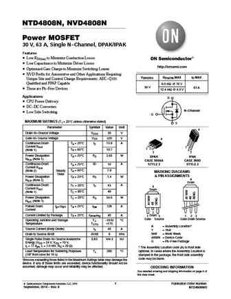
NTD4808N, NVD4808N Power MOSFET 30 V, 63 A, Single N-Channel, DPAK/IPAK Features Low RDS(on) to Minimize Conduction Losses Low Capacitance to Minimize Driver Losses http //onsemi.com Optimized Gate Charge to Minimize Switching Losses NVD Prefix for Automotive and Other Applications Requiring V(BR)DSS RDS(ON) MAX ID MAX Unique Site and Control Change Requirements; AEC-Q
9.8. Size:115K onsemi
nvd4856n.pdf
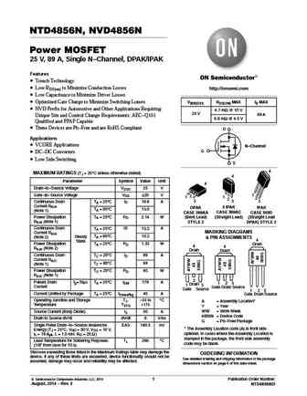
NTD4856N, NVD4856N Power MOSFET 25 V, 89 A, Single N-Channel, DPAK/IPAK Features Trench Technology Low RDS(on) to Minimize Conduction Losses http //onsemi.com Low Capacitance to Minimize Driver Losses Optimized Gate Charge to Minimize Switching Losses V(BR)DSS RDS(ON) MAX ID MAX NVD Prefix for Automotive and Other Applications Requiring 4.7 mW @ 10 V 25 V 89 A U
9.9. Size:89K onsemi
ntd4804n nvd4804n.pdf
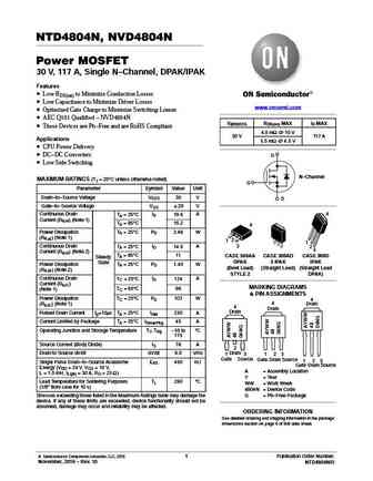
NTD4804N, NVD4804N Power MOSFET 30 V, 117 A, Single N-Channel, DPAK/IPAK Features Low RDS(on) to Minimize Conduction Losses Low Capacitance to Minimize Driver Losses www.onsemi.com Optimized Gate Charge to Minimize Switching Losses AEC Q101 Qualified - NVD4804N V(BR)DSS RDS(on) MAX ID MAX These Devices are Pb-Free and are RoHS Compliant 4.0 mW @ 10 V 30 V 117 A
Otros transistores... NVD3055-150, NVD3055L170, NVD4804N, NVD4805N, NVD4806N, NVD4808N, NVD4809N, NVD4810N, IRFB31N20D, NVD4856N, NVD4C05N, NVD5117PL, NVD5414N, NVD5484NL, NVD5490NL, NVD5802N, NVD5805N