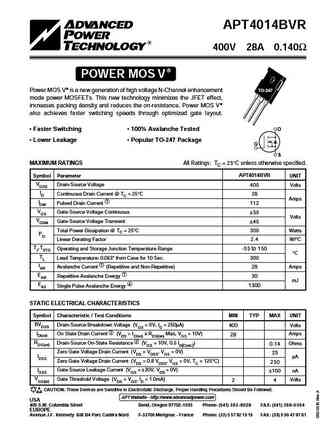
APT4018BN MOSFET Equivalente. Reemplazo. Hoja de especificaciones. Principales características
Número de Parte: APT4018BN
Tipo de FET: MOSFET
Polaridad de transistor: N
ESPECIFICACIONES MÁXIMAS
Pdⓘ - Máxima disipación de potencia: 360 W
|Vds|ⓘ - Voltaje máximo drenador-fuente: 400 V
|Vgs|ⓘ - Voltaje máximo fuente-puerta: 30 V
|Id|ⓘ - Corriente continua de drenaje: 29 A
Tjⓘ - Temperatura máxima de unión: 150 °C
CARACTERÍSTICAS ELÉCTRICAS
trⓘ - Tiempo de subida: 42 nS
Cossⓘ - Capacitancia de salida: 690 pF
RDSonⓘ - Resistencia estado encendido drenaje a fuente: 0.18 Ohm
Encapsulados: TO-247
Búsqueda de reemplazo de APT4018BN MOSFET
- Selecciónⓘ de transistores por parámetros
APT4018BN datasheet
apt4018bn.pdf

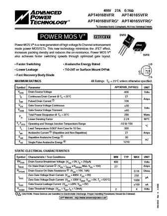
D TO-247 G APT4016BN 400V 31.0A 0.16 S APT4018BN 400V 29.0A 0.18 POWER MOS IV N- CHANNEL ENHANCEMENT MODE HIGH VOLTAGE POWER MOSFETS MAXIMUM RATINGS All Ratings TC = 25 C unless otherwise specified. APT APT Symbol Parameter 4016BN 4018BN UNIT VDSS Drain-Source Voltage 400 400 Volts ID Continuous Drain Current @ TC = 25 C 31 29 Amps IDM Pulsed Drain Current 1 124 116
apt4018hvr.pdf
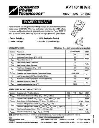
APT4018HVR 400V 22A 0.180 POWER MOS V TO-258 Power MOS V is a new generation of high voltage N-Channel enhancement mode power MOSFETs. This new technology minimizes the JFET effect, increases packing density and reduces the on-resistance. Power MOS V also achieves faster switching speeds through optimized gate layout. D Faster Switching 100% Avalanche Tested Lower
apt4012bvfrg apt4012svfrg.pdf
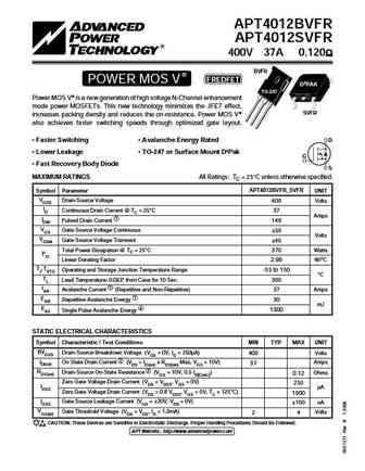
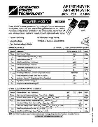
APT4012BVFR APT4012SVFR 400V 37A 0.120 BVFR FREDFET POWER MOS V D3PAK TO-247 Power MOS V is a new generation of high voltage N-Channel enhancement mode power MOSFETs. This new technology minimizes the JFET effect, SVFR increases packing density and reduces the on-resistance. Power MOS V also achieves faster switching speeds through optimized gate layout.
apt4016bn.pdf
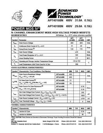
D TO-247 G APT4016BN 400V 31.0A 0.16 S APT4018BN 400V 29.0A 0.18 POWER MOS IV N- CHANNEL ENHANCEMENT MODE HIGH VOLTAGE POWER MOSFETS MAXIMUM RATINGS All Ratings TC = 25 C unless otherwise specified. APT APT Symbol Parameter 4016BN 4018BN UNIT VDSS Drain-Source Voltage 400 400 Volts ID Continuous Drain Current @ TC = 25 C 31 29 Amps IDM Pulsed Drain Current 1 124 116

Otros transistores... APT39F60J, APT39M60J, APT4012BVFRG, APT4012SVFRG, APT4014BVFRG, APT4014SVFRG, APT4016BVFRG, APT4016SVFRG, 8205A, APT4020BVFRG, APT4065BN, APT4080BN, APT40M35JVFR, APT40M70B2VFRG, APT40M70JVFR, APT40M70LVFRG, APT40N60B2CF
🌐 : EN ES РУ

Liste
Recientemente añadidas las descripciónes de los transistores:
MOSFET: FTF30P35D | FTF25N35DHVT | FTF15N35D | FTE15C35G | FTP02P15G | FTE02P15G | AKF30N5P0SX | AKF30N10S | AKF20P45D | CM4407 | CM3407 | CM3400 | SVF11N65F | SVF11N65T | FKBB3105 | EHBA036R1
Popular searches
17n80c3 | bc107 transistor | rjp63g4 datasheet | 2sc1115 | c3998 transistor | 2sa679 | 2sc3181 | 2sb324