APT4018BN. Аналоги и основные параметры
Наименование производителя: APT4018BN
Тип транзистора: MOSFET
Полярность: N
Предельные значения
Pd ⓘ
- Максимальная рассеиваемая мощность: 360 W
|Vds|ⓘ - Максимально допустимое напряжение сток-исток: 400 V
|Vgs|ⓘ - Максимально допустимое напряжение затвор-исток: 30 V
|Id| ⓘ - Максимально допустимый постоянный ток стока: 29 A
Tj ⓘ - Максимальная температура канала: 150 °C
Электрические характеристики
tr ⓘ -
Время нарастания: 42 ns
Cossⓘ - Выходная емкость: 690 pf
RDSonⓘ - Сопротивление сток-исток открытого транзистора: 0.18 Ohm
Тип корпуса: TO-247
Аналог (замена) для APT4018BN
- подборⓘ MOSFET транзистора по параметрам
APT4018BN даташит
..1. Size:36K apt
apt4018bn.pdf 

D TO-247 G APT4016BN 400V 31.0A 0.16 S APT4018BN 400V 29.0A 0.18 POWER MOS IV N- CHANNEL ENHANCEMENT MODE HIGH VOLTAGE POWER MOSFETS MAXIMUM RATINGS All Ratings TC = 25 C unless otherwise specified. APT APT Symbol Parameter 4016BN 4018BN UNIT VDSS Drain-Source Voltage 400 400 Volts ID Continuous Drain Current @ TC = 25 C 31 29 Amps IDM Pulsed Drain Current 1 124 116
7.1. Size:63K apt
apt4018hvr.pdf 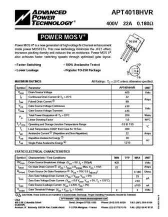
APT4018HVR 400V 22A 0.180 POWER MOS V TO-258 Power MOS V is a new generation of high voltage N-Channel enhancement mode power MOSFETs. This new technology minimizes the JFET effect, increases packing density and reduces the on-resistance. Power MOS V also achieves faster switching speeds through optimized gate layout. D Faster Switching 100% Avalanche Tested Lower
8.1. Size:73K apt
apt4012bvfrg apt4012svfrg.pdf 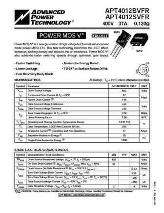
APT4012BVFR APT4012SVFR 400V 37A 0.120 BVFR FREDFET POWER MOS V D3PAK TO-247 Power MOS V is a new generation of high voltage N-Channel enhancement mode power MOSFETs. This new technology minimizes the JFET effect, SVFR increases packing density and reduces the on-resistance. Power MOS V also achieves faster switching speeds through optimized gate layout.
8.2. Size:52K apt
apt4016bn.pdf 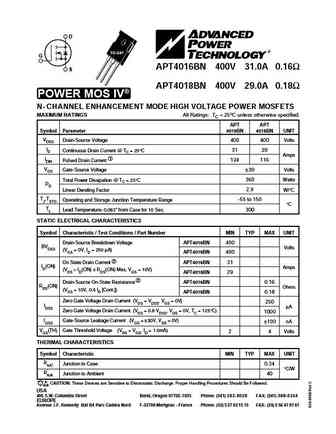
D TO-247 G APT4016BN 400V 31.0A 0.16 S APT4018BN 400V 29.0A 0.18 POWER MOS IV N- CHANNEL ENHANCEMENT MODE HIGH VOLTAGE POWER MOSFETS MAXIMUM RATINGS All Ratings TC = 25 C unless otherwise specified. APT APT Symbol Parameter 4016BN 4018BN UNIT VDSS Drain-Source Voltage 400 400 Volts ID Continuous Drain Current @ TC = 25 C 31 29 Amps IDM Pulsed Drain Current 1 124 116
8.3. Size:64K apt
apt4014bvr.pdf 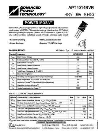
APT4014BVR 400V 28A 0.140 POWER MOS V Power MOS V is a new generation of high voltage N-Channel enhancement TO-247 mode power MOSFETs. This new technology minimizes the JFET effect, increases packing density and reduces the on-resistance. Power MOS V also achieves faster switching speeds through optimized gate layout. Faster Switching 100% Avalanche Tested D Lower L
8.4. Size:64K apt
apt4016bvr.pdf 
APT4016BVR 400V 27A 0.160 POWER MOS V Power MOS V is a new generation of high voltage N-Channel enhancement TO-247 mode power MOSFETs. This new technology minimizes the JFET effect, increases packing density and reduces the on-resistance. Power MOS V also achieves faster switching speeds through optimized gate layout. D Faster Switching 100% Avalanche Tested Lower
8.5. Size:72K apt
apt4014bvfrg apt4014svfrg.pdf 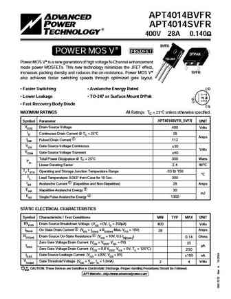
APT4014BVFR APT4014SVFR 400V 28A 0.140 BVFR FREDFET POWER MOS V D3PAK TO-247 Power MOS V is a new generation of high voltage N-Channel enhancement mode power MOSFETs. This new technology minimizes the JFET effect, SVFR increases packing density and reduces the on-resistance. Power MOS V also achieves faster switching speeds through optimized gate layout.
8.6. Size:65K apt
apt4012bvr.pdf 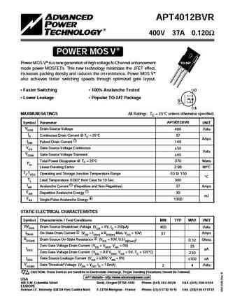
APT4012BVR 400V 37A 0.120 POWER MOS V Power MOS V is a new generation of high voltage N-Channel enhancement TO-247 mode power MOSFETs. This new technology minimizes the JFET effect, increases packing density and reduces the on-resistance. Power MOS V also achieves faster switching speeds through optimized gate layout. Faster Switching 100% Avalanche Tested D Lower L
8.7. Size:64K apt
apt4015avr.pdf 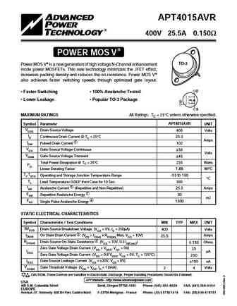
APT4015AVR 400V 25.5A 0.150 POWER MOS V TO-3 Power MOS V is a new generation of high voltage N-Channel enhancement mode power MOSFETs. This new technology minimizes the JFET effect, increases packing density and reduces the on-resistance. Power MOS V also achieves faster switching speeds through optimized gate layout. D Faster Switching 100% Avalanche Tested Lower
8.8. Size:64K apt
apt4014hvr.pdf 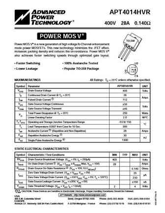
APT4014HVR 400V 28A 0.140 POWER MOS V TO-258 Power MOS V is a new generation of high voltage N-Channel enhancement mode power MOSFETs. This new technology minimizes the JFET effect, increases packing density and reduces the on-resistance. Power MOS V also achieves faster switching speeds through optimized gate layout. Faster Switching 100% Avalanche Tested D Lower
8.9. Size:72K apt
apt4016bvfrg apt4016svfrg.pdf 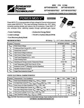
400V 27A 0.16 APT4016BVFR APT4016SVFR APT4016BVFRG* APT4016SVFRG* *G Denotes RoHS Compliant, Pb Free Terminal Finish. BVFR FREDFET POWER MOS V Power MOS V is a new generation of high voltage N-Channel enhancement D3PAK mode power MOSFETs. This new technology minimizes the JFET effect, increases packing density and reduces the on-resistance. Power MOS V SVF
8.10. Size:375K inchange semiconductor
apt4014bvfr.pdf 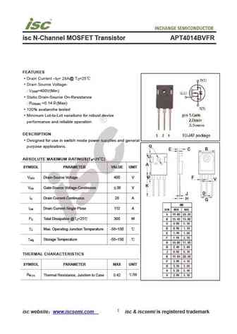
isc N-Channel MOSFET Transistor APT4014BVFR FEATURES Drain Current I = 28A@ T =25 D C Drain Source Voltage- V =400V(Min) DSS Static Drain-Source On-Resistance R =0.14 (Max) DS(on) 100% avalanche tested Minimum Lot-to-Lot variations for robust device performance and reliable operation DESCRIPTION Designed for use in switch mode power supplies and general pur
Другие IGBT... APT39F60J, APT39M60J, APT4012BVFRG, APT4012SVFRG, APT4014BVFRG, APT4014SVFRG, APT4016BVFRG, APT4016SVFRG, 8205A, APT4020BVFRG, APT4065BN, APT4080BN, APT40M35JVFR, APT40M70B2VFRG, APT40M70JVFR, APT40M70LVFRG, APT40N60B2CF
