30N50 Datasheet. Equivalente. Reemplazo. Hoja de especificaciones. Principales características
Número de Parte: 30N50 📄📄
Tipo de FET: MOSFET
Polaridad de transistor: N
ESPECIFICACIONES MÁXIMAS
Pdⓘ - Máxima disipación de potencia: 300 W
|Vds|ⓘ - Voltaje máximo drenador-fuente: 500 V
|Vgs|ⓘ - Voltaje máximo fuente-puerta: 20 V
|Id|ⓘ - Corriente continua de drenaje: 30 A
Tjⓘ - Temperatura máxima de unión: 150 °C
CARACTERÍSTICAS ELÉCTRICAS
RDSonⓘ - Resistencia estado encendido drenaje a fuente: 0.25 Ohm
Encapsulados: TO3PN
📄📄 Copiar
Búsqueda de reemplazo de 30N50 MOSFET
- Selecciónⓘ de transistores por parámetros
30N50 datasheet
..1. Size:211K inchange semiconductor
30n50.pdf 
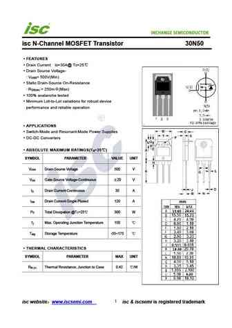
INCHANGE Semiconductor isc N-Channel MOSFET Transistor 30N50 FEATURES Drain Current I =30A@ T =25 D C Drain Source Voltage- V = 500V(Min) DSS Static Drain-Source On-Resistance R = 250m (Max) DS(on) 100% avalanche tested Minimum Lot-to-Lot variations for robust device performance and reliable operation APPLICATIONS Switch-Mode and Resonant-Mode Power Suppli
0.1. Size:237K motorola
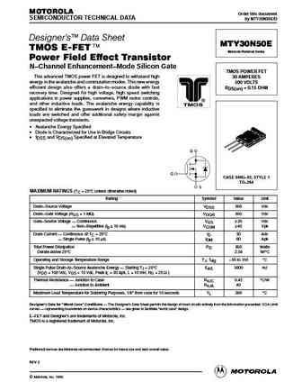
mty30n50erev2x.pdf 

MOTOROLA Order this document SEMICONDUCTOR TECHNICAL DATA by MTY30N50E/D Designer's Data Sheet MTY30N50E TMOS E-FET. Motorola Preferred Device Power Field Effect Transistor N Channel Enhancement Mode Silicon Gate TMOS POWER FET This advanced TMOS power FET is designed to withstand high 30 AMPERES energy in the avalanche and commutation modes. This new energy 500 VOLTS e
0.2. Size:197K motorola
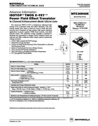
mte30n50e.pdf 

MOTOROLA Order this document SEMICONDUCTOR TECHNICAL DATA by MTE30N50E/D Advance Information MTE30N50E ISOTOP TMOS E-FET. Motorola Preferred Device Power Field Effect Transistor N Channel Enhancement Mode Silicon Gate TMOS POWER FET 30 AMPERES This advanced TMOS E FET is designed to withstand high 500 VOLTS energy in the avalanche mode and switch efficiently. This new
0.3. Size:229K motorola
mte30n50erev0a.pdf 

MOTOROLA Order this document SEMICONDUCTOR TECHNICAL DATA by MTE30N50E/D Advance Information MTE30N50E ISOTOP TMOS E-FET. Motorola Preferred Device Power Field Effect Transistor N Channel Enhancement Mode Silicon Gate TMOS POWER FET 30 AMPERES This advanced TMOS E FET is designed to withstand high 500 VOLTS energy in the avalanche mode and switch efficiently. This new
0.4. Size:204K motorola
mty30n50e.pdf 

MOTOROLA Order this document SEMICONDUCTOR TECHNICAL DATA by MTY30N50E/D Designer's Data Sheet MTY30N50E TMOS E-FET. Motorola Preferred Device Power Field Effect Transistor N Channel Enhancement Mode Silicon Gate TMOS POWER FET This advanced TMOS power FET is designed to withstand high 30 AMPERES energy in the avalanche and commutation modes. This new energy 500 VOLTS e
0.6. Size:1207K rohm
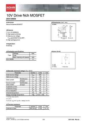
zdx130n50.pdf 

Data Sheet 10V Drive Nch MOSFET ZDX130N50 Structure Dimensions (Unit mm) TO-220FM TO-220FM Silicon N-channel MOSFET 10.0 3.2 4.5 10.0 3.2 4.5 2.8 2.8 Features 1) Low on-resistance. 1.2 1.2 1.3 1.3 2) High-speed switching. 3) Gate-source voltage 0.8 0.8 2.54 2.54 0.75 2.6 2.54 2.54 0.75 2.6 VGSS guaranteed to be 30V . (1) (2) (3) (1) (2) (3) 4) Hig
0.7. Size:142K ixys
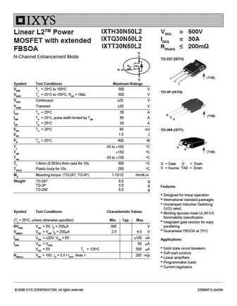
ixth30n50l2-ixtq30n50l2-ixtt30n50l2.pdf 

IXTH30N50L2 VDSS = 500V Linear L2TM Power IXTQ30N50L2 ID25 = 30A MOSFET with extended IXTT30N50L2 RDS(on) 200m FBSOA D D D D O D O N-Channel Enhancement Mode TO-247 (IXTH) RGi w w G O O (TAB) S Symbol Test Conditions Maximum Ratings VDSS TJ = 25 C to 150 C 500 V TO-3P (IXTQ) VDGR TJ = 25 C to 150 C, RGS = 1M 500 V VGSS Continu
0.8. Size:320K ixys
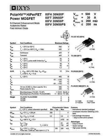
ixfh30n50p ixft30n50p ixfv30n50p.pdf 

VDSS = 500 V IXFH 30N50P PolarHVTM HiPerFET ID25 = 30 A IXFT 30N50P Power MOSFET RDS(on) 200 m IXFV 30N50P N-Channel Enhancement Mode trr 200 ns IXFV 30N50PS Avalanche Rated Fast Intrinsic Diode TO-247 AD (IXFH) Symbol Test Conditions Maximum Ratings VDSS TJ = 25 C to 150 C 500 V D (TAB) VDGR TJ = 25 C to
0.9. Size:110K ixys
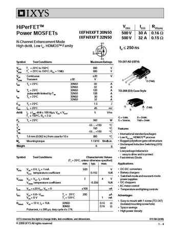
ixfh30n50 ixfh32n50 ixft30n50 ixft32n50.pdf 

VDSS ID25 RDS(on) HiPerFETTM IXFH/IXFT 30N50 500 V 30 A 0.16 W Power MOSFETs IXFH/IXFT 32N50 500 V 32 A 0.15 W N-Channel Enhancement Mode High dv/dt, Low trr, HDMOSTM Family trr 250 ns TO-247 AD (IXFH) Symbol Test Conditions Maximum Ratings VDSS TJ = 25 C to 150 C 500 V VDGR TJ = 25 C to 150 C; RGS = 1 MW 500 V VGS Continuous 20 V VGSM Transient 30 V D (TAB) ID25 TC
0.10. Size:109K ixys
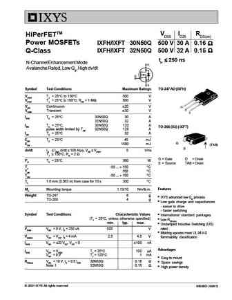
ixft30n50q.pdf 

VDSS ID25 RDS(on) HiPerFETTM Power MOSFETs IXFH/IXFT 30N50Q 500 V 30 A 0.16 IXFH/IXFT 32N50Q 500 V 32 A 0.15 Q-Class trr 250 ns N-Channel Enhancement Mode Avalanche Rated, Low Qg, High dv/dt Symbol Test Conditions Maximum Ratings TO-247 AD (IXFH) VDSS TJ = 25 C to 150 C 500 V VDGR TJ = 25 C to 150 C; RGS =
0.11. Size:336K ixys
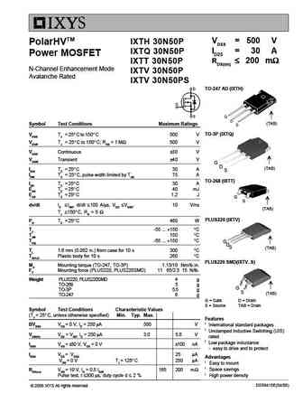
ixth30n50p ixtq30n50p ixtt30n50p ixtv30n50p.pdf 

VDSS = 500 V IXTH 30N50P PolarHVTM ID25 = 30 A IXTQ 30N50P Power MOSFET RDS(on) 200 m IXTT 30N50P N-Channel Enhancement Mode IXTV 30N50P Avalanche Rated IXTV 30N50PS TO-247 AD (IXTH) (TAB) Symbol Test Conditions Maximum Ratings TO-3P (IXTQ) VDSS TJ = 25 C to 150 C 500 V VDGR TJ = 25 C to 150 C; RGS = 1 M 500 V VGSS Continuo
0.12. Size:123K ixys
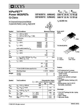
ixfk30n50q ixfx30n50q.pdf 

VDSS ID25 RDS(on) HiPerFETTM IXFK/IXFX 30N50Q 500 V 30 A 0.16 Power MOSFETs IXFK/IXFX 32N50Q 500 V 32 A 0.15 Q-Class trr 250 ns N-Channel Enhancement Mode Avalanche Rated, Low Qg, High dv/dt Symbol Test Conditions Maximum Ratings PLUS 247TM (IXFX) VDSS TJ = 25 C to 150 C 500 V VDGR TJ = 25 C to 150 C; RGS
0.13. Size:40K ixys
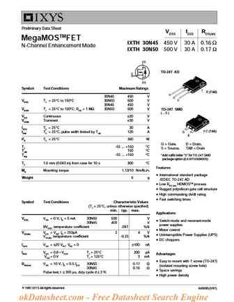
ixth30n45 ixth30n50.pdf 

Preliminary Data Sheet VDSS ID25 RDS(on) MegaMOSTMFET IXTH 30N45 450 V 30 A 0.16 N-Channel Enhancement Mode IXTH 30N50 500 V 30 A 0.17 TO-247 AD Symbol Test Conditions Maximum Ratings D (TAB) 30N45 450 V VDSS TJ = 25 C to 150 C 30N50 500 V 30N45 450 V VDGR TJ = 25 C to 150 C; RGS = 1 M 30N50 500 V TO-247 SMD ( ...S ) VGS Continuous 20 V VGSM Transient 30 V ID
0.14. Size:109K ixys
ixfh30n50q.pdf 

VDSS ID25 RDS(on) HiPerFETTM IXFH/IXFT 30N50 500 V 30 A 0.16 W Power MOSFETs IXFH/IXFT 32N50 500 V 32 A 0.15 W N-Channel Enhancement Mode High dv/dt, Low trr, HDMOSTM Family trr 250 ns TO-247 AD (IXFH) Symbol Test Conditions Maximum Ratings VDSS TJ = 25 C to 150 C 500 V VDGR TJ = 25 C to 150 C; RGS = 1 MW 500 V VGS Continuous 20 V VGSM Transient 30 V D (TAB) ID25 TC
0.15. Size:91K ixys
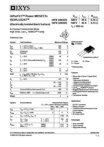
ixfr30n50q ixfr32n50q.pdf 

VDSS ID25 RDS(on) HiPerFETTM Power MOSFETs ISOPLUS247TM IXFR 30N50Q 500 V 29 A 0.16 W IXFR 32N50Q 500 V 30 A 0.15 W (Electrically Isolated Back Surface) trr 250 ns N-Channel Enhancement Mode High dV/dt, Low trr, HDMOSTM Family Preliminary data ISOPLUS 247TM Symbol Test Conditions Maximum Ratings E 153432 VDSS TJ = 25 C to 150 C 500 V VDGR TJ = 25 C to 150 C; RGS = 1 MW 500 V
0.16. Size:196K onsemi
mty30n50e.pdf 

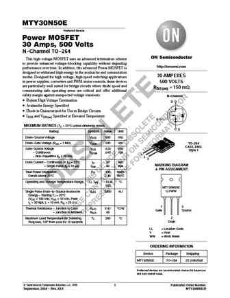
MTY30N50E Preferred Device Power MOSFET 30 Amps, 500 Volts N-Channel TO-264 This high voltage MOSFET uses an advanced termination scheme to provide enhanced voltage-blocking capability without degrading http //onsemi.com performance over time. In addition, this advanced Power MOSFET is designed to withstand high energy in the avalanche and commutation 30 AMPERES modes. Designed for h
0.17. Size:1368K belling
bl30n50-w bl30n50-f.pdf 

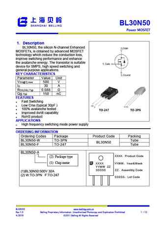
BL30N50 Power MOSFET 1 Description BL30N50, the silicon N-channel Enhanced MOSFETs, is obtained by advanced MOSFET technology which reduce the conduction loss, improve switching performance and enhance the avalanche energy. The transistor is suitable device for SMPS, high speed switching and general purpose applications. KEY CHARACTERISTICS Parameter Value Unit V 500
0.18. Size:1020K jiaensemi
jfhm30n50p.pdf 

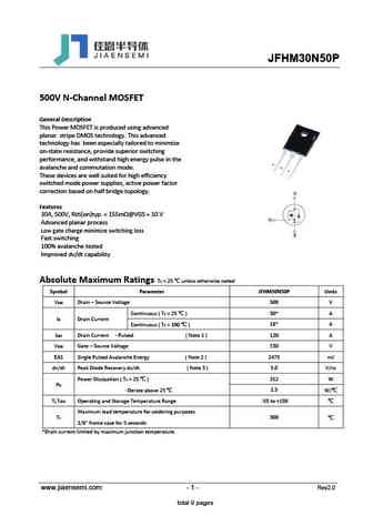
JFHM30N50P 500V N-Channel MOSFET General Description This Power MOSFET is produced using advanced planar stripe DMOS technology. This advanced technology has been especially tailored to minimize on-state resistance, provide superior switching performance, and withstand high energy pulse in the avalanche and commutation mode. These devices are well suited for high efficiency
0.19. Size:724K jiaensemi
jfam30n50e.pdf 

JFAM30N50E 500V N-Channel MOSFET General Description This Power MOSFET is produced using advanced planar stripe DMOS technology. This advanced technology has been especially tailored to minimize on-state resistance, provide superior switching performance, and withstand high energy pulse in the avalanche and commutation mode. These devices are well suited for high efficiency
0.20. Size:750K pipsemi
ptw30n50el.pdf 

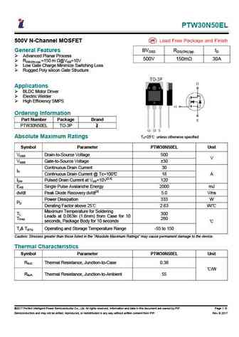
PTW30N50EL 500V N-Channel MOSFET General Features BVDSS RDS(ON),typ. ID Advanced Planar Process 500V 150m 30A RDS(ON),typ.=150 m @VGS=10V Low Gate Charge Minimize Switching Loss Rugged Poly silicon Gate Structure Applications BLDC Motor Driver Electric Welder High Efficiency SMPS Ordering Information Part Number Package Brand PTW30N5
0.21. Size:494K cn fx-semi
fxn30n50f.pdf 

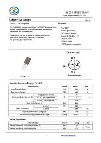
FuXin Semiconductor Co., Ltd. FXN30N50F Series Rev.A General Description Features The FXN30N50F uses advanced Silicon s MOSFET Technology, which V = 500V DS provides high performance in on-state resistance, fast switching ID =30A @V = 10V GS performance, and excellent quality. Very low on-resistance These devices can also be utilized in industrial ap
0.22. Size:624K cn fx-semi
fxn30n50t.pdf 

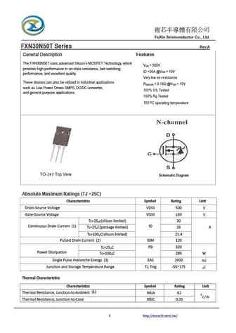
FuXin Semiconductor Co., Ltd. FXN30N50T Series Rev.A General Description Features The FXN30N50T uses advanced Silicon s MOSFET Technology, which V = 500V DS provides high performance in on-state resistance, fast switching ID =30A @V = 10V GS performance, and excellent quality. Very low on-resistance These devices can also be utilized in industrial ap
0.23. Size:211K inchange semiconductor
ixth30n50l.pdf 
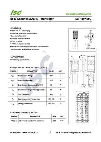
INCHANGE Semiconductor isc N-Channel MOSFET Transistor IXTH30N50L FEATURES With TO-247 packaging With low gate drive requirements Low switching loss Low on-state resistance Easy to drive 100% avalanche tested Minimum Lot-to-Lot variations for robust device performance and reliable operation APPLICATIONS Switching applications ABSOLUTE MAXIMUM RATINGS(T =25 )
Otros transistores... NTGD3147FT1G, NTGD3148NT1G, 2SK1085-M, 2SK1969-01, 2SK2258, 2SK2753, 2SK3262, 2SK428, STP80NF70, 80N06, AM30N10, AOD2144, BUK437-500B, BUK637-500B, CSD30N30, FCH067N65S3, FCP067N65S3


