NTP6412ANG MOSFET. Datasheet. Equivalente. Reemplazo. Hoja de especificaciones. Principales características
Número de Parte: NTP6412ANG
Código: 6412AN
Tipo de FET: MOSFET
Polaridad de transistor: N
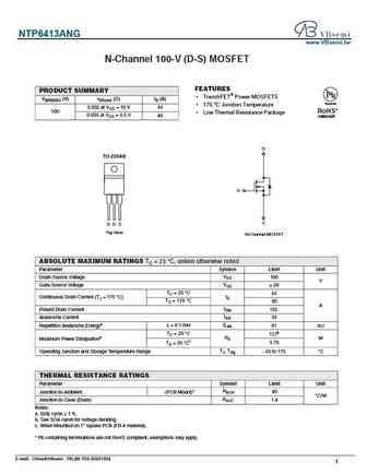
ESPECIFICACIONES MÁXIMAS
Máxima disipación de potencia (Pd): 167 W
Voltaje máximo drenador - fuente |Vds|: 100 V
Voltaje máximo fuente - puerta |Vgs|: 20 V
Corriente continua de drenaje |Id|: 58 A
Temperatura máxima de unión (Tj): 175 °C
CARACTERÍSTICAS ELÉCTRICAS
Tensión umbral entre puerta y fuente |Vgs(th)|: 4 V
Carga de la puerta (Qg): 73 nC
Tiempo de subida (tr): 140 nS
Conductancia de drenaje-sustrato (Cd): 400 pF
Resistencia entre drenaje y fuente RDS(on): 0.0182 Ohm
Paquete / Cubierta: TO-220
Búsqueda de reemplazo de MOSFET NTP6412ANG
NTP6412ANG Datasheet (PDF)
ntb6412ang ntp6412ang.pdf
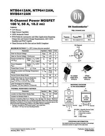
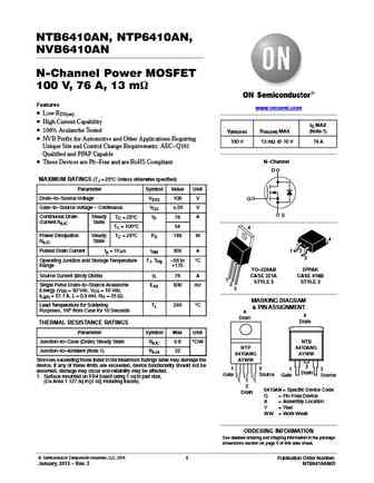
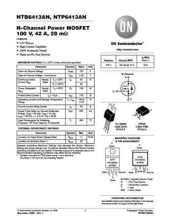
![](https://alltransistors.com/ad/pdf_icon.gif)
NTB6412AN, NTP6412AN,NVB6412ANN-Channel Power MOSFET100 V, 58 A, 18.2 mWFeatures Low RDS(on)http://onsemi.com High Current Capability 100% Avalanche TestedID MAX NVB Prefix for Automotive and Other Applications Requiring V(BR)DSS RDS(ON) MAX (Note 1)Unique Site and Control Change Requirements; AEC-Q101100 V 18.2 mW @ 10 V 58 AQualified and PPAP Capable
ntb6412an ntp6412an nvb6412an.pdf
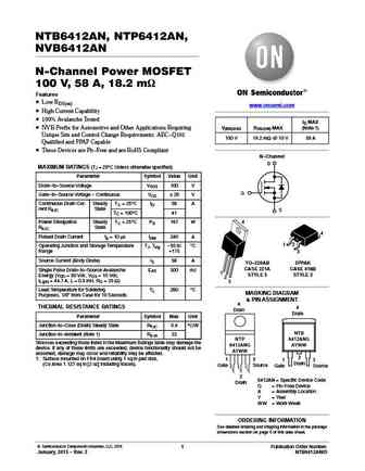
![](https://alltransistors.com/ad/pdf_icon.gif)
NTB6412AN, NTP6412AN,NVB6412ANN-Channel Power MOSFET100 V, 58 A, 18.2 mWFeatures Low RDS(on)www.onsemi.com High Current Capability 100% Avalanche TestedID MAX NVB Prefix for Automotive and Other Applications Requiring V(BR)DSS RDS(ON) MAX (Note 1)Unique Site and Control Change Requirements; AEC-Q101100 V 18.2 mW @ 10 V 58 AQualified and PPAP Capable Th
ntb6412an ntp6412an.pdf
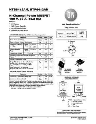
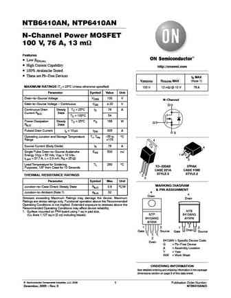
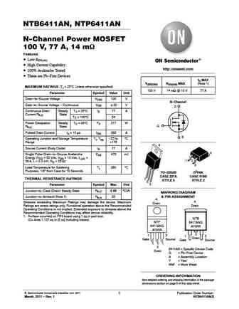
![](https://alltransistors.com/ad/pdf_icon.gif)
NTB6412AN, NTP6412ANN-Channel Power MOSFET100 V, 58 A, 18.2 mWFeatures Low RDS(on) High Current Capabilityhttp://onsemi.com 100% Avalanche Tested These are Pb-Free DevicesID MAXV(BR)DSS RDS(ON) MAX (Note 1)MAXIMUM RATINGS (TJ = 25C Unless otherwise specified)100 V 18.2 mW @ 10 V 58 AParameter Symbol Value UnitDrain-to-Source Voltage VDSS 100 VN-Channe
ntb6413ang ntp6413ang.pdf
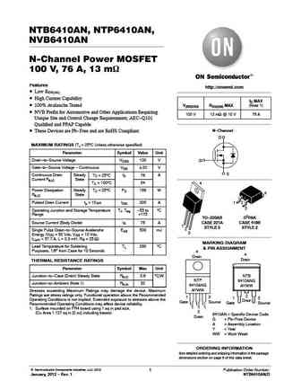
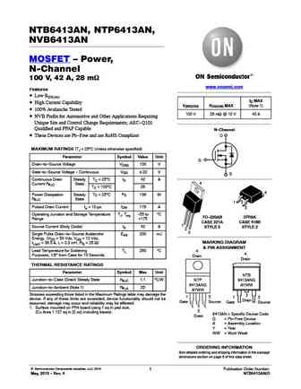
![](https://alltransistors.com/ad/pdf_icon.gif)
NTB6413AN, NTP6413AN,NVB6413ANN-Channel Power MOSFET100 V, 42 A, 28 mWFeatures Low RDS(on)http://onsemi.com High Current Capability 100% Avalanche TestedID MAX NVB Prefix for Automotive and Other Applications Requiring V(BR)DSS RDS(ON) MAX (Note 1)Unique Site and Control Change Requirements; AEC-Q101100 V 28 mW @ 10 V 42 AQualified and PPAP Capable The
ntb6410ang ntp6410ang.pdf
![](https://alltransistors.com/ad/pdf_icon.gif)
NTB6410AN, NTP6410AN,NVB6410ANN-Channel Power MOSFET100 V, 76 A, 13 mWFeatureshttp://onsemi.com Low RDS(on) High Current CapabilityID MAX 100% Avalanche TestedV(BR)DSS RDS(ON) MAX (Note 1) NVB Prefix for Automotive and Other Applications Requiring100 V 13 mW @ 10 V 76 AUnique Site and Control Change Requirements; AEC-Q101Qualified and PPAP CapableN-Chan
ntb6410an ntp6410an.pdf
![](https://alltransistors.com/ad/pdf_icon.gif)
NTB6410AN, NTP6410ANN-Channel Power MOSFET100 V, 76 A, 13 mWFeatures Low RDS(on) High Current Capabilityhttp://onsemi.com 100% Avalanche Tested These are Pb-Free DevicesID MAXV(BR)DSS RDS(ON) MAX (Note 1)MAXIMUM RATINGS (TJ = 25C Unless otherwise specified)100 V 13 mW @ 10 V 76 AParameter Symbol Value UnitDrain-to-Source Voltage VDSS 100 VN-ChannelG
ntb6411n ntp6411n.pdf
![](https://alltransistors.com/ad/pdf_icon.gif)
NTB6411AN, NTP6411ANN-Channel Power MOSFET100 V, 77 A, 14 mWFeatures Low RDS(on) High Current Capabilityhttp://onsemi.com 100% Avalanche Tested These are Pb-Free DevicesID MAXV(BR)DSS RDS(ON) MAX (Note 1)MAXIMUM RATINGS (TJ = 25C Unless otherwise specified)100 V 14 mW @ 10 V 77 AParameter Symbol Value UnitDrain-to-Source Voltage VDSS 100 VN-ChannelG
ntb6410an ntp6410an nvb6410an.pdf
![](https://alltransistors.com/ad/pdf_icon.gif)
NTB6410AN, NTP6410AN,NVB6410ANN-Channel Power MOSFET100 V, 76 A, 13 mWFeatureswww.onsemi.com Low RDS(on) High Current CapabilityID MAX 100% Avalanche TestedV(BR)DSS RDS(ON) MAX (Note 1) NVB Prefix for Automotive and Other Applications Requiring100 V 13 mW @ 10 V 76 AUnique Site and Control Change Requirements; AEC-Q101Qualified and PPAP CapableN-Channel
ntb6413an ntp6413an nvb6413an.pdf
![](https://alltransistors.com/ad/pdf_icon.gif)
NTB6413AN, NTP6413AN,NVB6413ANMOSFET Power,N-Channel100 V, 42 A, 28 mWwww.onsemi.comFeatures Low RDS(on)ID MAX High Current CapabilityV(BR)DSS RDS(ON) MAX (Note 1) 100% Avalanche Tested100 V 28 mW @ 10 V 42 A NVB Prefix for Automotive and Other Applications RequiringUnique Site and Control Change Requirements; AEC-Q101Qualified and PPAP CapableN-C
ntp6411ang.pdf
![](https://alltransistors.com/ad/pdf_icon.gif)
NTB6411AN, NTP6411ANN-Channel Power MOSFET100 V, 77 A, 14 mWFeatures Low RDS(on) High Current Capabilityhttp://onsemi.com 100% Avalanche Tested These are Pb-Free DevicesID MAXV(BR)DSS RDS(ON) MAX (Note 1)MAXIMUM RATINGS (TJ = 25C Unless otherwise specified)100 V 14 mW @ 10 V 77 AParameter Symbol Value UnitDrain-to-Source Voltage VDSS 100 VN-ChannelG
ntb6413an ntp6413an.pdf
![](https://alltransistors.com/ad/pdf_icon.gif)
NTB6413AN, NTP6413ANN-Channel Power MOSFET100 V, 42 A, 28 mWFeatures Low RDS(on) High Current Capabilityhttp://onsemi.com 100% Avalanche Tested These are Pb-Free DevicesID MAXV(BR)DSS RDS(ON) MAX (Note 1)MAXIMUM RATINGS (TJ = 25C Unless otherwise specified)100 V 28 mW @ 10 V 42 AParameter Symbol Value UnitDrain-to-Source Voltage VDSS 100 VN-ChannelG
ntp6413ang.pdf
![](https://alltransistors.com/ad/pdf_icon.gif)
NTP6413ANGwww.VBsemi.twN-Channel 100-V (D-S) MOSFETFEATURESPRODUCT SUMMARY TrenchFET Power MOSFETSV(BR)DSS (V) rDS(on) ()ID (A)Available 175 C Junction Temperature0.032 at VGS = 10 V45RoHS*100 Low Thermal Resistance Package0.035 at VGS = 4.5 V40COMPLIANTDTO-220AB GSG D STop ViewN-Channel MOSFETABSOLUTE MAXIMUM RATINGS TC = 25 C,
Otros transistores... FQT7N10L , FDP083N15A , FQU10N20C , FDP075N15A , FQU11P06 , FQU12N20 , FDPF085N10A , FQU13N06L , IRF540N , FDB86102LZ , FQU17P06 , FQU1N60C , FDP085N10A , FQU20N06L , FQU2N100 , FQU2N60C , FDMC8030 .