6N90A MOSFET Equivalente. Reemplazo. Hoja de especificaciones. Principales características
Número de Parte: 6N90A
Tipo de FET: MOSFET
Polaridad de transistor: N
ESPECIFICACIONES MÁXIMAS
Pdⓘ - Máxima disipación de potencia: 167 W
|Vds|ⓘ - Voltaje máximo drenador-fuente: 900 V
|Vgs|ⓘ - Voltaje máximo fuente-puerta: 30 V
|Id|ⓘ - Corriente continua de drenaje: 6 A
Tjⓘ - Temperatura máxima de unión: 150 °C
CARACTERÍSTICAS ELÉCTRICAS
trⓘ - Tiempo de subida: 90 nS
Cossⓘ - Capacitancia de salida: 110 pF
RDSonⓘ - Resistencia estado encendido drenaje a fuente: 2.3 Ohm
Encapsulados: TO-220AB
Búsqueda de reemplazo de 6N90A MOSFET
- Selecciónⓘ de transistores por parámetros
6N90A datasheet
6n90a 6n90af.pdf
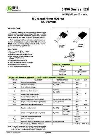
RoHS 6N90 Series RoHS SEMICONDUCTOR Nell High Power Products N-Channel Power MOSFET 6A, 900Volts DESCRIPTION D The Nell 6N90 is a three-terminal silicon device with current conduction capability of 6A, fast switching speed, low on-state resistance, breakdown voltage rating of 900V, and max. threshold voltage of 5 volts. They are designed for use in applications such as G DS G
ssh6n90a.pdf
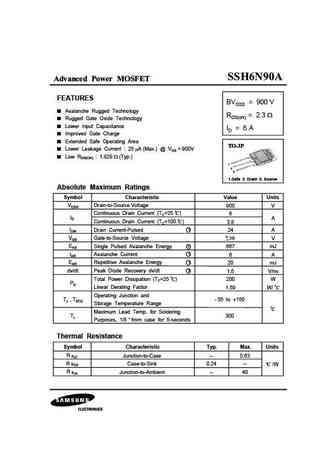
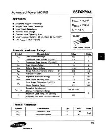
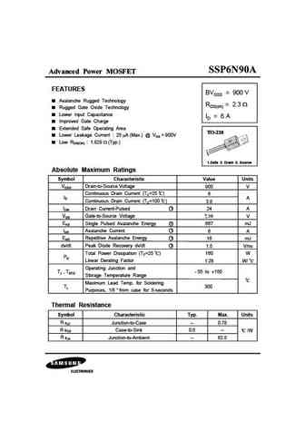
Advanced Power MOSFET FEATURES BVDSS = 900 V Avalanche Rugged Technology RDS(on) = 2.3 Rugged Gate Oxide Technology Lower Input Capacitance ID = 6 A Improved Gate Charge Extended Safe Operating Area Lower Leakage Current 25 A (Max.) @ VDS = 900V Low RDS(ON) 1.829 (Typ.) 1 2 3 1.Gate 2. Drain 3. Source Absolute Maximum Ratings Symbol Characteristic Value
sss6n90a.pdf
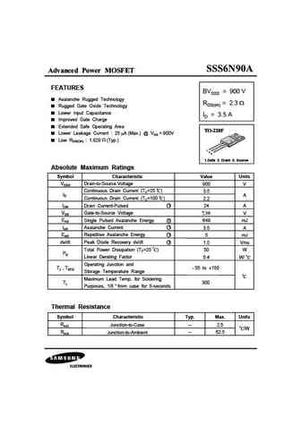
Advanced Power MOSFET FEATURES BVDSS = 900 V Avalanche Rugged Technology RDS(on) = 2.3 Rugged Gate Oxide Technology Lower Input Capacitance ID = 3.5 A Improved Gate Charge Extended Safe Operating Area Lower Leakage Current 25 A (Max.) @ VDS = 900V Low RDS(ON) 1.829 (Typ.) 1 2 3 1.Gate 2. Drain 3. Source Absolute Maximum Ratings Symbol Characteristic Value
Otros transistores... 6HP04MH, 6LN04SS, 6N60A, 6N60AF, 6N60F, 6N60G, 6N80A, 6N80AF, STF13NM60N, 6N90AF, 75N08, 75N10A, 75N10B, MSAFA75N10C, MSAFX76N07A, 7N60AF, 7N60H
History: TSM1N60LCP | BL5N135-A
🌐 : EN ES РУ

Liste
Recientemente añadidas las descripciónes de los transistores:
MOSFET: AUP060N055 | AUP056N10 | AUP056N08BGL | AUP052N085 | AUP045N12 | AUP039N10 | AUP034N10 | AUP034N06 | AUP033N08BG | AUP026N085 | AUN084N10 | AUN065N10 | AUN063N10 | AUN062N08BG | AUN060N08AG | AUN053N10
Popular searches
c3306 datasheet | hy3810 | c711 transistor | k3599 transistor datasheet | 2sc1735 | transistor 2sc5200 | 2sb560 transistor | a1273