6N90A Datasheet. Specs and Replacement
Type Designator: 6N90A 📄📄
Type of Transistor: MOSFET
Type of Control Channel: N-Channel
Absolute Maximum Ratings
Pd ⓘ - Maximum Power Dissipation: 167 W
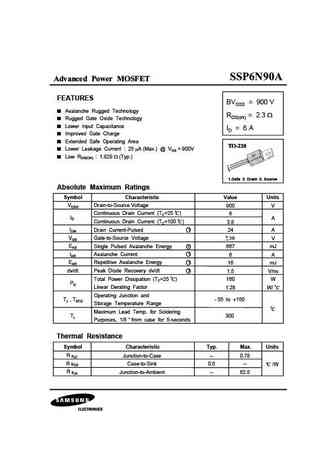
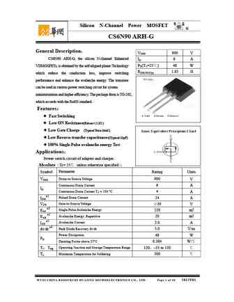
|Vds|ⓘ - Maximum Drain-Source Voltage: 900 V
|Vgs|ⓘ - Maximum Gate-Source Voltage: 30 V
|Id| ⓘ - Maximum Drain Current: 6 A
Tj ⓘ - Maximum Junction Temperature: 150 °C
Electrical Characteristics
tr ⓘ - Rise Time: 90 nS
Cossⓘ - Output Capacitance: 110 pF
RDSonⓘ - Maximum Drain-Source On-State Resistance: 2.3 Ohm
Package: TO-220AB
📄📄 Copy
6N90A substitution
- MOSFET ⓘ Cross-Reference Search
6N90A datasheet
6n90a 6n90af.pdf
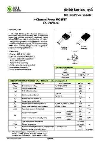
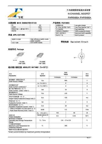
RoHS 6N90 Series RoHS SEMICONDUCTOR Nell High Power Products N-Channel Power MOSFET 6A, 900Volts DESCRIPTION D The Nell 6N90 is a three-terminal silicon device with current conduction capability of 6A, fast switching speed, low on-state resistance, breakdown voltage rating of 900V, and max. threshold voltage of 5 volts. They are designed for use in applications such as G DS G... See More ⇒
ssh6n90a.pdf
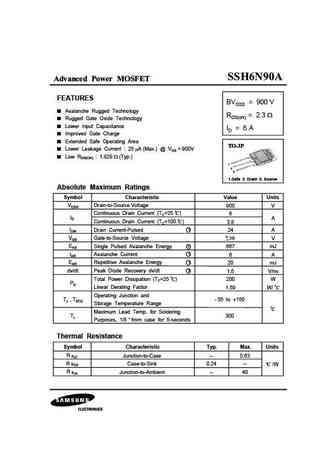
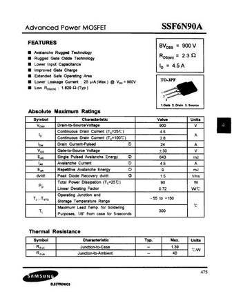
Advanced Power MOSFET FEATURES BVDSS = 900 V Avalanche Rugged Technology RDS(on) = 2.3 Rugged Gate Oxide Technology Lower Input Capacitance ID = 6 A Improved Gate Charge Extended Safe Operating Area Lower Leakage Current 25 A (Max.) @ VDS = 900V Low RDS(ON) 1.829 (Typ.) 1 2 3 1.Gate 2. Drain 3. Source Absolute Maximum Ratings Symbol Characteristic Value ... See More ⇒
sss6n90a.pdf
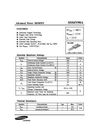
Advanced Power MOSFET FEATURES BVDSS = 900 V Avalanche Rugged Technology RDS(on) = 2.3 Rugged Gate Oxide Technology Lower Input Capacitance ID = 3.5 A Improved Gate Charge Extended Safe Operating Area Lower Leakage Current 25 A (Max.) @ VDS = 900V Low RDS(ON) 1.829 (Typ.) 1 2 3 1.Gate 2. Drain 3. Source Absolute Maximum Ratings Symbol Characteristic Value ... See More ⇒
Detailed specifications: 6HP04MH, 6LN04SS, 6N60A, 6N60AF, 6N60F, 6N60G, 6N80A, 6N80AF, HY1906P, 6N90AF, 75N08, 75N10A, 75N10B, MSAFA75N10C, MSAFX76N07A, 7N60AF, 7N60H
Keywords - 6N90A MOSFET specs
6N90A cross reference
6N90A equivalent finder
6N90A pdf lookup
6N90A substitution
6N90A replacement
Learn how to find the right MOSFET substitute. A guide to cross-reference, check specs and replace MOSFETs in your circuits.
MOSFET Parameters. How They Affect Each Other
History: 3N210
🌐 : EN ES РУ

LIST
Last Update
MOSFET: CS95118 | CS85105A | CS75N45 | CS72N12 | CS55N50 | CS48N75A | CS40N27 | MSQ60P04D | MSQ40P07D | MSQ30P40D
Popular searches
c3306 datasheet | hy3810 | c711 transistor | k3599 transistor datasheet | 2sc1735 | transistor 2sc5200 | 2sb560 transistor | a1273