IRFS4510 MOSFET Equivalente. Reemplazo. Hoja de especificaciones. Principales características
Número de Parte: IRFS4510
Tipo de FET: MOSFET
Polaridad de transistor: N
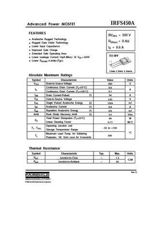
ESPECIFICACIONES MÁXIMAS
Pdⓘ - Máxima disipación de potencia: 140 W
|Vds|ⓘ - Voltaje máximo drenador-fuente: 100 V
|Vgs|ⓘ - Voltaje máximo fuente-puerta: 20 V
|Id|ⓘ - Corriente continua de drenaje: 61 A
Tjⓘ - Temperatura máxima de unión: 175 °C
CARACTERÍSTICAS ELÉCTRICAS
trⓘ - Tiempo de subida: 32 nS
Cossⓘ - Capacitancia de salida: 220 pF
RDSonⓘ - Resistencia estado encendido drenaje a fuente: 0.0139 Ohm
Búsqueda de reemplazo de IRFS4510 MOSFET
- Selecciónⓘ de transistores por parámetros
IRFS4510 datasheet
irfs4510pbf irfsl4510pbf.pdf
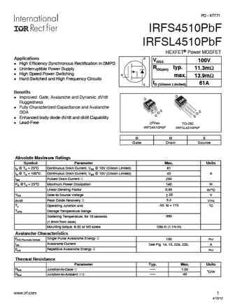
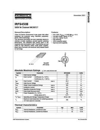
PD - 97771 IRFS4510PbF IRFSL4510PbF HEXFET Power MOSFET D Applications VDSS 100V l High Efficiency Synchronous Rectification in SMPS RDS(on) typ. 11.3m l Uninterruptible Power Supply l High Speed Power Switching G max. 13.9m l Hard Switched and High Frequency Circuits ID (Silicon Limited) 61A S Benefits D l Improved Gate, Avalanche and Dynamic dV/dt D Ruggedness l
irfs4510.pdf
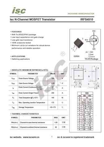
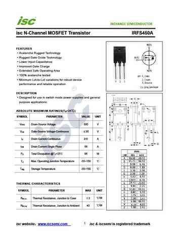
Isc N-Channel MOSFET Transistor IRFS4510 FEATURES With To-263(D2PAK) package Low input capacitance and gate charge Low gate input resistance 100% avalanche tested Minimum Lot-to-Lot variations for robust device performance and reliable operation APPLICATIONS Switching applications ABSOLUTE MAXIMUM RATINGS(T =25 ) a SYMBOL PARAMETER VALUE UNIT V Drain-Source Volt
Otros transistores... IPS70R1K4CE, IPS70R950CE, IPU050N03L, IPU060N03L, IPU075N03L, IPU135N03L, IPU60R3K4CE, IRF135S203, SKD502T, IRFS7434, IRFS7437, IRFS7530, IRFS7537, IRFS7540, IRFS7730, IRFS7734, IRFS7762
🌐 : EN ES РУ

Liste
Recientemente añadidas las descripciónes de los transistores:
MOSFET: AUP060N055 | AUP056N10 | AUP056N08BGL | AUP052N085 | AUP045N12 | AUP039N10 | AUP034N10 | AUP034N06 | AUP033N08BG | AUP026N085 | AUN084N10 | AUN065N10 | AUN063N10 | AUN062N08BG | AUN060N08AG | AUN053N10
Popular searches
mje15032 | tip32c datasheet | mje15032g | irf1404 | bc550 | irf9530 | 2n2222a transistor | irfp250