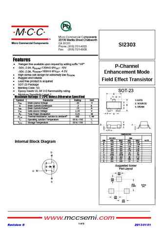
2303 MOSFET Equivalente. Reemplazo. Hoja de especificaciones. Principales características
Número de Parte: 2303
Tipo de FET: MOSFET
Polaridad de transistor: P
ESPECIFICACIONES MÁXIMAS
Pdⓘ - Máxima disipación de potencia: 0.35 W
|Vds|ⓘ - Voltaje máximo drenador-fuente: 30 V
|Vgs|ⓘ - Voltaje máximo fuente-puerta: 20 V
|Id|ⓘ - Corriente continua de drenaje: 1.9 A
Tjⓘ - Temperatura máxima de unión: 150 °C
CARACTERÍSTICAS ELÉCTRICAS
trⓘ - Tiempo de subida: 11 nS
Cossⓘ - Capacitancia de salida: 35 pF
RDSonⓘ - Resistencia estado encendido drenaje a fuente: 0.19 Ohm
Encapsulados: SOT-23
Búsqueda de reemplazo de 2303 MOSFET
- Selecciónⓘ de transistores por parámetros
2303 datasheet
rn2301 rn2302 rn2303 rn2304 rn2305 rn2306.pdf
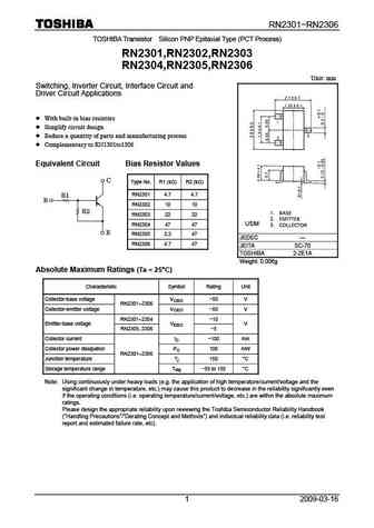
RN2301 RN2306 TOSHIBA Transistor Silicon PNP Epitaxial Type (PCT Process) RN2301,RN2302,RN2303 RN2304,RN2305,RN2306 Unit mm Switching, Inverter Circuit, Interface Circuit and Driver Circuit Applications With built-in bias resistors Simplify circuit design Reduce a quantity of parts and manufacturing process Complementary to RN1301to1306 Equivalent Circuit Bias Resi
si2303cds.pdf
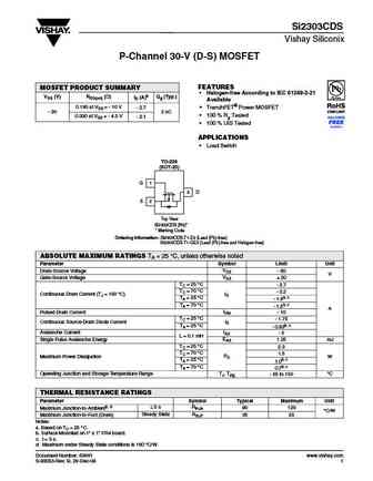
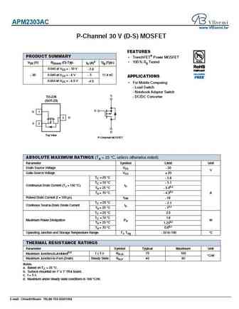
Si2303CDS Vishay Siliconix P-Channel 30-V (D-S) MOSFET FEATURES MOSFET PRODUCT SUMMARY Halogen-free According to IEC 61249-2-21 VDS (V) RDS(on) ( ) ID (A)a Qg (Typ.) Available 0.190 at VGS = - 10 V - 2.7 TrenchFET Power MOSFET - 30 2 nC 100 % Rg Tested 0.330 at VGS = - 4.5 V - 2.1 100 % UIS Tested APPLICATIONS Load Switch TO-236 (SOT-23) G 1 3 D
si2303ds.pdf
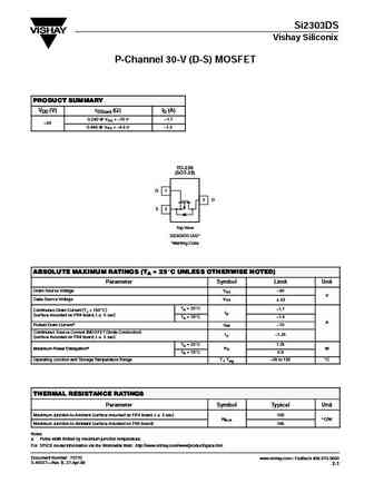
Si2303DS Vishay Siliconix P-Channel 30-V (D-S) MOSFET PRODUCT SUMMARY VDS (V) rDS(on) (W) ID (A) 0.240 @ VGS = 10 V 1.7 30 30 0.460 @ VGS = 4.5 V 1.3 TO-236 (SOT-23) G 1 3 D S 2 Top View Si2303DS (A3)* *Marking Code ABSOLUTE MAXIMUM RATINGS (TA = 25_C UNLESS OTHERWISE NOTED) Parameter Symbol Limit Unit Drain-Source Voltage VDS 30 V V Gate-Source Volta
sq2303es.pdf
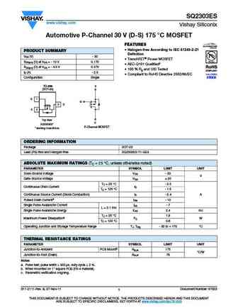
SQ2303ES www.vishay.com Vishay Siliconix Automotive P-Channel 30 V (D-S) 175 C MOSFET FEATURES Halogen-free According to IEC 61249-2-21 PRODUCT SUMMARY Definition VDS (V) - 30 TrenchFET Power MOSFET RDS(on) ( ) at VGS = - 10 V 0.170 AEC-Q101 Qualifiedc RDS(on) ( ) at VGS = - 4.5 V 0.370 100 % Rg and UIS Tested ID (A) - 2.5 Compliant to RoHS Directive 2
si2303bds.pdf
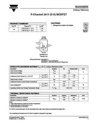
Si2303BDS Vishay Siliconix P-Channel 30-V (D-S) MOSFET FEATURES PRODUCT SUMMARY Halogen-free Option Available VDS (V) RDS(on) ( ) ID (A)b Pb-free 0.200 at VGS = - 10 V Available - 1.64 - 30 0.380 at VGS = - 4.5 V RoHS* - 1.0 COMPLIANT TO-236 (SOT-23) G 1 3 D S 2 Top View Si2303BDS (L3)* * Marking Code Ordering Information Si2303BDS-T1 Si2303BDS-T1-E3 (Lead (Pb)-
si2303cd.pdf

Si2303CDS Vishay Siliconix P-Channel 30-V (D-S) MOSFET FEATURES MOSFET PRODUCT SUMMARY Halogen-free According to IEC 61249-2-21 VDS (V) RDS(on) ( ) ID (A)a Qg (Typ.) Available 0.190 at VGS = - 10 V - 2.7 TrenchFET Power MOSFET - 30 2 nC 100 % Rg Tested 0.330 at VGS = - 4.5 V - 2.1 100 % UIS Tested APPLICATIONS Load Switch TO-236 (SOT-23) G 1 3 D
tsm2303cx.pdf
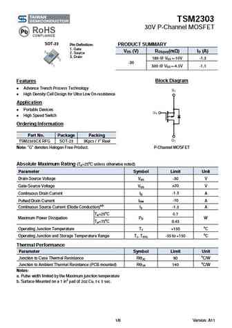
TSM2303 30V P-Channel MOSFET SOT-23 PRODUCT SUMMARY Pin Definition 1. Gate VDS (V) RDS(on)(m ) ID (A) 2. Source 3. Drain 180 @ VGS =-10V -1.3 -30 300 @ VGS =-4.5V -1.1 Block Diagram Features Advance Trench Process Technology High Density Cell Design for Ultra Low On-resistance Application Portable Devices High Speed Switch Ordering Info
cj2303.pdf
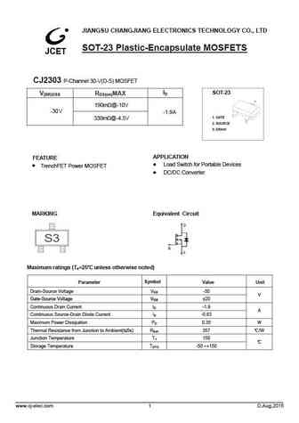
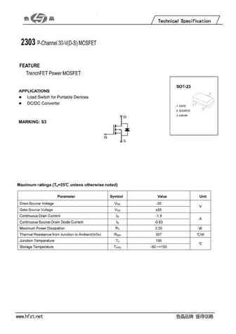
JIANGSU CHANGJIANG ELECTRONICS TECHNOLOGY CO., LTD SOT-23 Plastic-Encapsulate MOSFETS CJ2303 P-Channel 30-V(D-S) MOSFET ID SOT-23 V(BR)DSS RDS(on)MAX 190m @-10V -30V -1.9A 1. GATE 330m @-4.5V 2. SOURCE 3. DRAIN APPLICATION FEATURE Load Switch for Portable Devices TrenchFET Power MOSFET DC/DC Converter MARKING Equivalent Circuit Maximum ratings (Ta=
ku2303k.pdf
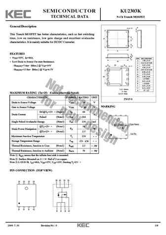
SEMICONDUCTOR KU2303K TECHNICAL DATA N-Ch Trench MOSFET General Description This Trench MOSFET has better characteristics, such as fast switching time, low on resistance, low gate charge and excellent avalanche characteristics. It is mainly suitable for DC/DC Converter. FEATURES VDSS=30V, ID=66A. Low Drain to Source On-state Resistance. RDS(ON)=7.4m (Max.) @ VGS=10V RDS(ON)
ku2303d.pdf
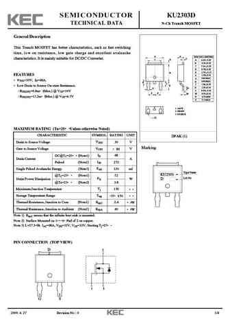
SEMICONDUCTOR KU2303D TECHNICAL DATA N-Ch Trench MOSFET General Description This Trench MOSFET has better characteristics, such as fast switching time, low on resistance, low gate charge and excellent avalanche A K DIM MILLIMETERS L characteristics. It is mainly suitable for DC/DC Converter. C D _ A 6.60 + 0.20 _ B 6.10 + 0.20 _ C 5.34 + 0.30 _ D 0.70 + 0.20 _ E 2.70 + 0.15
ku2303q.pdf
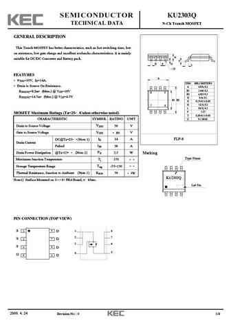
SEMICONDUCTOR KU2303Q TECHNICAL DATA N-Ch Trench MOSFET GENERAL DESCRIPTION This Trench MOSFET has better characteristics, such as fast switching time, low on resistance, low gate charge and excellent avalanche characteristiscs. It is mainly H suitable for DC/DC Converter and Battery pack. T D P G L U FEATURES A VDSS=30V, ID=14A. DIM MILLIMETERS Drain to Source On Resistance
ces2303.pdf
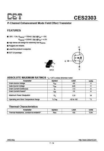
CES2303 P-Channel Enhancement Mode Field Effect Transistor FEATURES -30V, -1.9A, RDS(ON) = 150m (typ) @VGS = -10V. RDS(ON) = 230m (typ) @VGS = -4.5V. High dense cell design for extremely low RDS(ON). Rugged and reliable. D Lead free product is acquired. SOT-23 package. G D S G S SOT-23 ABSOLUTE MAXIMUM RATINGS TA = 25 C unless otherwise noted Parameter Symbol Limit Units
ced2303 ceu2303.pdf
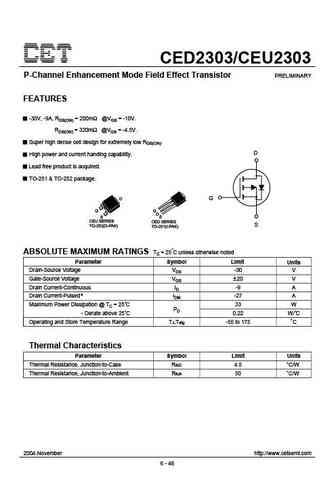
CED2303/CEU2303 P-Channel Enhancement Mode Field Effect Transistor PRELIMINARY FEATURES -30V, -9A, RDS(ON) = 200m @VGS = -10V. RDS(ON) = 320m @VGS = -4.5V. Super high dense cell design for extremely low RDS(ON). D High power and current handing capability. Lead free product is acquired. TO-251 & TO-252 package. D G G S CEU SERIES CED SERIES S TO-252(D-PAK) TO-251(I-PAK)
se2303.pdf
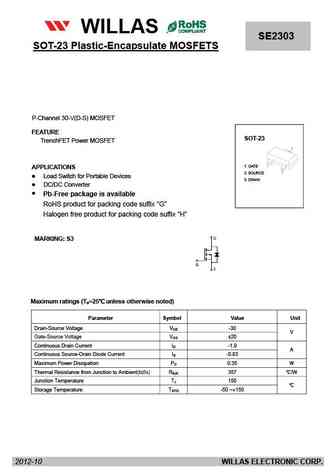
FM120-M WILLAS THRU SE2303 SOT-23 Plastic-Encapsulate MOSFETS FM1200-M 1.0A SURFACE MOUNT SCHOTTKY BARRIER RECTIFIERS -20V- 200V SOD-123 PACKAGE Pb Free Produ Package outline Features Batch process design, excellent power dissipation offers better reverse leakage current and thermal resistance. SOD-123H Low profile surface mounted application in order to optimize
aons32303.pdf
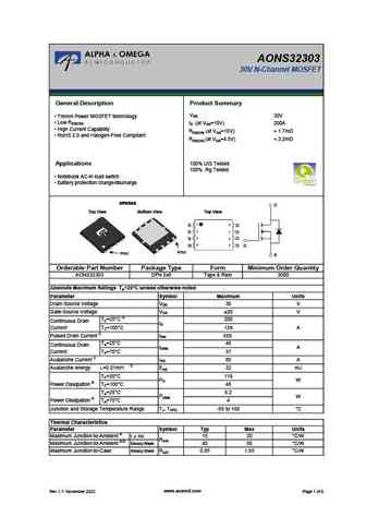
AONS32303 30V N-Channel MOSFET General Description Product Summary VDS 30V Trench Power MOSFET technology Low RDS(ON) ID (at VGS=10V) 200A High Current Capability RDS(ON) (at VGS=10V)
ap2303gn-hf.pdf
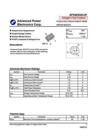
AP2303GN-HF Halogen-Free Product Advanced Power P-CHANNEL ENHANCEMENT MODE Electronics Corp. POWER MOSFET Simple Drive Requirement BVDSS -30V Small Package Outline RDS(ON) 240m D Surface Mount Device ID - 1.9A RoHS Compliant & Halogen-Free S SOT-23 G Description D Advanced Power MOSFETs from APEC provide the designer with the best combination of fast switching,
ap2303gn.pdf
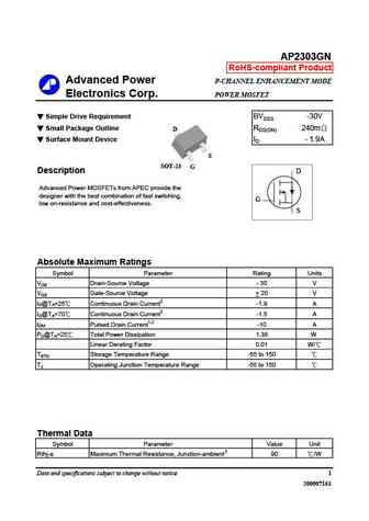
AP2303GN RoHS-compliant Product Advanced Power P-CHANNEL ENHANCEMENT MODE Electronics Corp. POWER MOSFET Simple Drive Requirement BVDSS -30V Small Package Outline RDS(ON) 240m D Surface Mount Device ID - 1.9A S SOT-23 G Description D Advanced Power MOSFETs from APEC provide the designer with the best combination of fast switching, G low on-resistance and cost-effect
am2303p.pdf
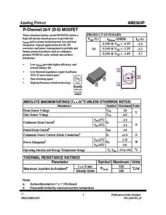
Analog Power AM2303P P-Channel 20-V (D-S) MOSFET PRODUCT SUMMARY These miniature surface mount MOSFETs utilize a high cell density trench process to provide low VDS (V) rDS(on) (OHM) ID (A) rDS(on) and to ensure minimal power loss and heat 0.100 @ VGS = -4.5V -2.9 dissipation. Typical applications are DC-DC converters and power management in portable and -20 0.160 @ VGS = -2.5V -
afp2303a.pdf
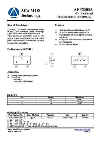
AFP2303A Alfa-MOS 30V P-Channel Technology Enhancement Mode MOSFET General Description Features AFP2303A, P-Channel enhancement mode -30V/-2.8A,RDS(ON)=145m @VGS=-10.0V MOSFET, uses Advanced Trench Technology -30V/-2.4A,RDS(ON)=180m @VGS=-4.5V to provide excellent RDS(ON), low gate charge. Super high density cell design for extremely These devices are particularly
afp2303.pdf
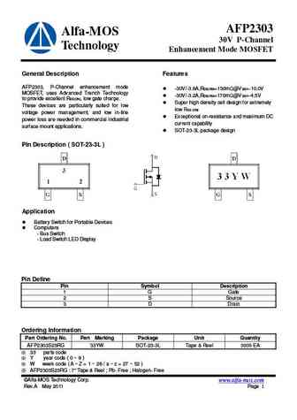
AFP2303 Alfa-MOS 30V P-Channel Technology Enhancement Mode MOSFET General Description Features AFP2303, P-Channel enhancement mode -30V/-3.6A,RDS(ON)=130m @VGS=-10.0V MOSFET, uses Advanced Trench Technology -30V/-3.2A,RDS(ON)=170m @VGS=-4.5V to provide excellent RDS(ON), low gate charge. Super high density cell design for extremely These devices are particularly s
si2303.pdf
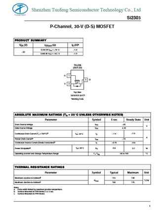
Shenzhen Tuofeng Semiconductor Technology Co., Ltd Si2303 P-Channel, 30-V (D-S) MOSFET PRODUCT SUMMARY VDS (V) rDS(on) (W) ID (A)b 0.240 @ VGS = 10 V 1.4 30 0.460 @ VGS = 4.5 V 1.0 TO-236 (SOT-23) G 1 3 D S 2 Top View Si2303DS (A3T)* *Marking Code ABSOLUTE MAXIMUM RATINGS (TA = 25_C UNLESS OTHERWISE NOTED) Parameter Symbol 5 sec Steady State Unit Drain-Source V
mtp2303n3.pdf
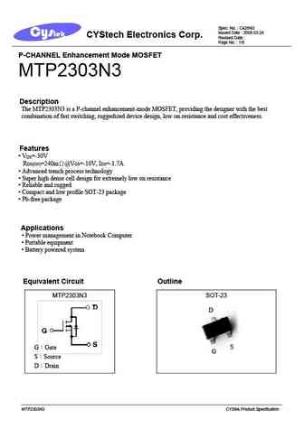
Spec. No. C426N3 Issued Date 2008.03.24 CYStech Electronics Corp. Revised Date Page No. 1/8 P-CHANNEL Enhancement Mode MOSFET MTP2303N3 Description The MTP2303N3 is a P-channel enhancement-mode MOSFET, providing the designer with the best combination of fast switching, ruggedized device design, low on-resistance and cost effectiveness. Features V =-30V DS
brcs2303ma.pdf
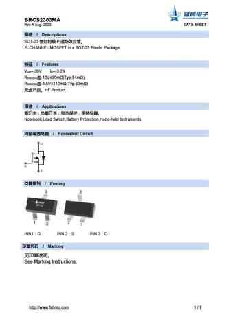
BRCS2303MA Rev.A Aug.-2023 DATA SHEET / Descriptions SOT-23 P P- CHANNEL MOSFET in a SOT-23 Plastic Package. / Features V =-30V I =-3.2A DS D R DS(ON)@-10V 90m (Typ.54m ) R DS(ON)@-4.5V 110m (Typ.63m ) HF Product. / Applications Not
sm2303psa.pdf
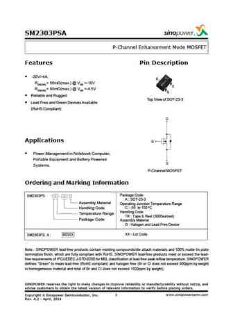
SM2303PSA P-Channel Enhancement Mode MOSFET Features Pin Description -30V/-4A, D RDS(ON) = 56m (max.) @ VGS =-10V S RDS(ON) = 88m (max.) @ VGS =-4.5V G Reliable and Rugged Top View of SOT-23-3 Lead Free and Green Devices Available (RoHS Compliant) D Applications G Power Management in Notebook Computer, Portable Equipment and Battery Powered S Systems. P-Channel MOSFE
apm2303a.pdf
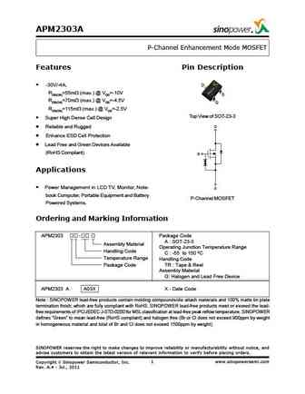
APM2303A P-Channel Enhancement Mode MOSFET Features Pin Description -30V/-4A, D RDS(ON)=55m (max.) @ VGS=-10V S RDS(ON)=70m (max.) @ VGS=-4.5V G RDS(ON)=115m (max.) @ VGS=-2.5V Top View of SOT-23-3 Super High Dense Cell Design D Reliable and Rugged Enhance ESD Cell Protection Lead Free and Green Devices Available (RoHS Compliant) G Applications P
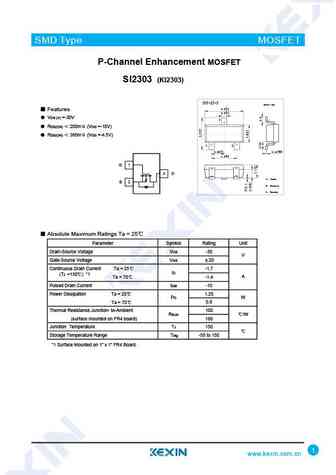
ki2303ds.pdf
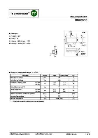
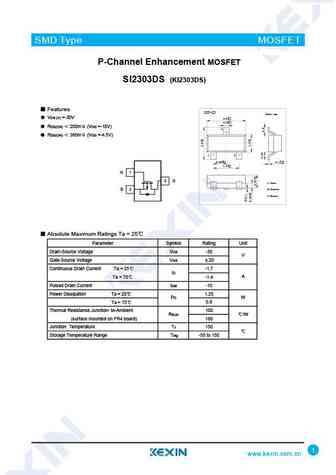
SMD Type IC SMD Type MOSFE SMD Type MOSFET SMD Type MOSFET SMD Type MOSFET SMD Type IC Product specification KI2303 DS SOT-23 Unit mm +0.1 2.9-0.1 Features +0.1 0.4-0.1 VDS (V) = -30V 3 ID = -1.4 A RDS(ON)
si2303ds-3.pdf
SMD Type MOSFET P-Channel Enhancement MOSFET SI2303DS (KI2303DS) SOT-23-3 Unit mm +0.2 2.9-0.1 Features +0.1 0.4 -0.1 VDS (V) =-30V 3 RDS(ON) 200m (VGS =-10V) RDS(ON) 380m (VGS =-4.5V) 1 2 +0.02 +0.1 0.15 -0.02 0.95 -0.1 +0.1 1.9 -0.2 G 1 3 D 1. Gate S 2 2. Source 3. Drain Absolute Maximum Ratings Ta = 25 Parameter Symbol Ratin
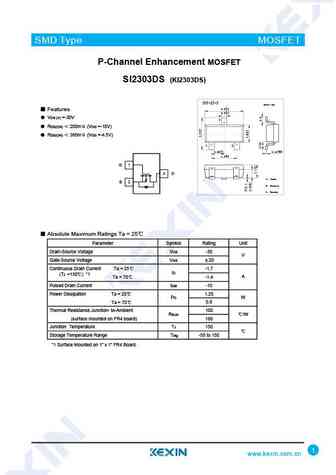
si2303ds.pdf
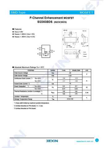
SMD Type MOSFET P-Channel Enhancement MOSFET SI2303DS (KI2303DS) Features SOT-23 Unit mm +0.1 VDS (V) =-30V 2.9 -0.1 +0.1 0.4-0.1 RDS(ON) 200m (VGS =-10V) 3 RDS(ON) 380m (VGS =-4.5V) 1 2 +0.1 +0.05 0.95 -0.1 0.1 -0.01 +0.1 1.9 -0.1 G 1 3 D 1.Gate 2.Source S 2 3.Drain Absolute Maximum Ratings Ta = 25 Parameter Symbol Rating Unit
si2303bds.pdf
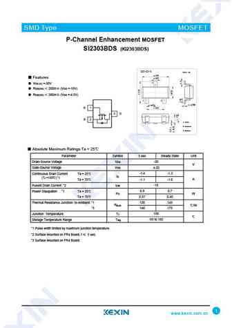
SMD Type MOSFET P-Channel Enhancement MOSFET SI2303BDS (KI2303BDS) Features SOT-23 Unit mm +0.1 VDS (V) =-30V 2.9 -0.1 +0.1 0.4 -0.1 RDS(ON) 200m (VGS =-10V) 3 RDS(ON) 380m (VGS =-4.5V) 1 2 +0.1 +0.05 0.95-0.1 0.1-0.01 +0.1 1.9-0.1 G 1 3 D 1.Gate S 2 2.Source 3.Drain Absolute Maximum Ratings Ta = 25 Parameter Symbol 5 sec Steady
ki2303bds.pdf
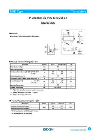
SMD Type Transistors P-Channel, 30-V (G-S) MOSFET KI2303BDS SOT-23 Unit mm +0.1 2.9-0.1 +0.1 0.4-0.1 Features 3 RoH Lead (Pb)-Free Version is RoHS Compliant. 12 +0.1 +0.05 0.95-0.1 0.1-0.01 +0.1 1.9-0.1 1.Base 1. Gate 2.Emitter 2. Source 3. Drain 3.collector Absolute Maximum Ratings Ta = 25 Parameter Symbol 5 sec Steady State Unit Drain-Source Voltage VDS -30 V Gate-
si2303bds-3.pdf
SMD Type MOSFET P-Channel Enhancement MOSFET SI2303BDS (KI2303BDS) SOT-23-3 Unit mm +0.2 2.9 -0.1 +0.1 Features 0.4 -0.1 3 VDS (V) =-30V RDS(ON) 200m (VGS =-10V) RDS(ON) 380m (VGS =-4.5V) 1 2 +0.02 +0.1 0.15 -0.02 0.95-0.1 +0.1 G 1 1.9-0.2 3 D S 2 1.Gate 2.Source 3.Drain Absolute Maximum Ratings Ta = 25 Parameter Symbol 5 sec St
si2303 ki2303.pdf
SMD Type MOSFET P-Channel Enhancement MOSFET SI2303 (KI2303) SOT-23-3 Unit mm +0.2 2.9-0.1 Features +0.1 0.4 -0.1 VDS (V) =-30V 3 RDS(ON) 200m (VGS =-10V) RDS(ON) 380m (VGS =-4.5V) 1 2 +0.02 +0.1 0.15 -0.02 0.95 -0.1 +0.1 1.9 -0.2 G 1 3 D 1. Gate S 2 2. Source 3. Drain Absolute Maximum Ratings Ta = 25 Parameter Symbol Rating Un
am2303.pdf
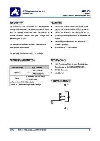
AiT Semiconductor Inc. AM2303 www.ait-ic.com MOSFET -30V P-CHANNEL ENHANCEMENT MODE DESCRIPTION FEATURES The AM2303 is the P-Channel logic enhancement -30V/-4.3A, R =50m (typ.)@V =-10V DS(ON) GS mode power field effect transistor is produced using -30V/-3.5A, R =58m (typ.)@V =-4.5V DS(ON) GS high cell density. advanced trench technology to -30V/-2.5A, R =73m (typ.
cht2303gp.pdf
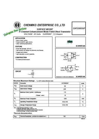
CHENMKO ENTERPRISE CO.,LTD CHT2303GP SURFACE MOUNT P-Channel Enhancement Mode Field Effect Transistor VOLTAGE 30 Volts CURRENT 1.9 Ampere APPLICATION * Servo motor control. * Power MOSFET gate drivers. * Other switching applications. SC-59/SOT-346 FEATURE * Small flat package. (SC-59 ) * High density cell design for extremely low RDS(ON). * Rugged and reliable. (2) * High sat
ctp2303.pdf
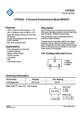
CTP2303 Crownpo Technology CTP2303 P-Channel Enhancement Mode MOSFET Features Description -30V/-1.7A,RDS(ON)=240 m @VGS=- 10V The CTP2303 is the P-Channel logic enhancement -30V/-1.3A,R =460 m @VGS=-4.5V mode power field effect transistors are produced using DS(ON) high cell density , DMOS trench technology. Super high density cell design for extremely low RDS(O
gsm2303a.pdf
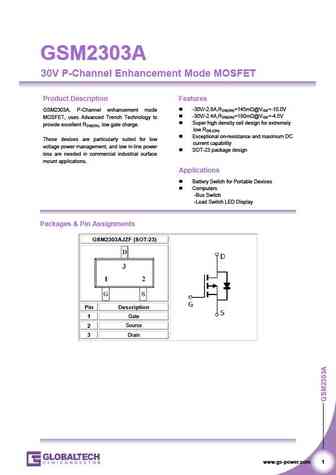
GSM2303A GSM2303A 30V P-Channel Enhancement Mode MOSFET Product Description Features -30V/-2.8A,RDS(ON)=145m @VGS=-10.0V GSM2303A, P-Channel enhancement mode -30V/-2.4A,RDS(ON)=180m @VGS=-4.5V MOSFET, uses Advanced Trench Technology to Super high density cell design for extremely provide excellent RDS(ON), low gate charge. low RDS (ON) Exceptional on-res
gsm2303.pdf
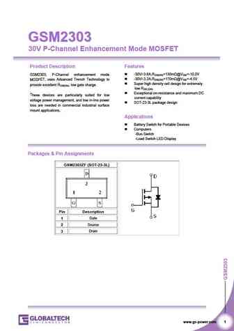
GSM2303 GSM2303 30V P-Channel Enhancement Mode MOSFET Product Description Features -30V/-3.6A,RDS(ON)=130m @VGS=-10.0V GSM2303, P-Channel enhancement mode -30V/-3.2A,RDS(ON)=170m @VGS=-4.5V MOSFET, uses Advanced Trench Technology to Super high density cell design for extremely provide excellent RDS(ON), low gate charge. low RDS (ON) Exceptional on-resist
me2303 me2303-g.pdf
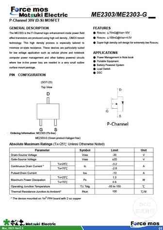
ME2303/ME2303-G P-Channel 30V (D-S) MOSFET GENERAL DESCRIPTION FEATURES The ME2303 is the P-Channel logic enhancement mode power field RDS(ON) 75m @VGS=-10V effect transistors are produced using high cell density , DMOS trench RDS(ON) 100m @VGS=-4.5V technology. This high density process is especially tailored to Super high density cell design for extremely low RDS(
nce2303.pdf
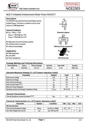
Pb Free Product http //www.ncepower.com NCE2303 NCE P-Channel Enhancement Mode Power MOSFET Description D The NCE2303 uses advanced trench technology to provide excellent RDS(ON), This device is suitable for use as a load G switch or in PWM applications. S General Features VDS = -30V,ID = -2.0A Schematic diagram RDS(ON)
shd230303.pdf
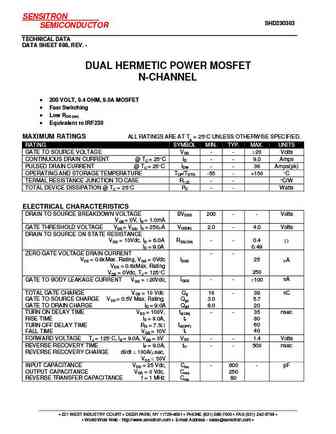
SENSITRON SHD230303 SEMICONDUCTOR TECHNICAL DATA DATA SHEET 698, REV. - DUAL HERMETIC POWER MOSFET N-CHANNEL 200 VOLT, 0.4 OHM, 9.0A MOSFET Fast Switching Low RDS (on) Equivalent to IRF230 MAXIMUM RATINGS ALL RATINGS ARE AT TA = 25 C UNLESS OTHERWISE SPECIFIED. RATING SYMBOL MIN. TYP. MAX. UNITS GATE TO SOURCE VOLTAGE VGS - - 20 Volts ID - - 9.0 Amps CONTINUOUS
shd230302.pdf
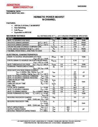
SENSITRON SHD230302 SEMICONDUCTOR TECHNICAL DATA DATA SHEET 602, REV - HERMETIC POWER MOSFET N-CHANNEL FEATURES 100 Volt, 0.18 Ohm, 7.4A MOSFET Fast Switching Low RDS (on) Equivalent to IRFE130 MAXIMUM RATINGS ALL RATINGS ARE AT TC = 25 C UNLESS OTHERWISE SPECIFIED. RATING SYMBOL MIN. TYP. MAX. UNITS GATE TO SOURCE VOLTAGE VGS - - 20 Volts ID - - 10.8 Amps O
ssm2303gn.pdf
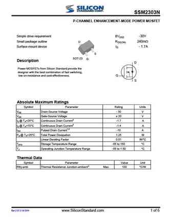
SSM2303N P-CHANNEL ENHANCEMENT-MODE POWER MOSFET Simple drive requirement BVDSS -30V Small package outline RDS(ON) 240m D Surface-mount device ID - 1.7A S SOT-23 G Description D Power MOSFETs from Silicon Standard provide the designer with the best combination of fast switching, low on-resistance and cost-effectiveness. G S Absolute Maximum Ratings Symbol Parameter Rating Un
st2303srg.pdf
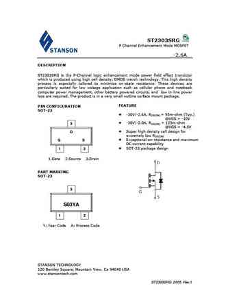
ST2303SRG P Channel Enhancement Mode MOSFET -2.6A DESCRIPTION ST2303SRG is the P-Channel logic enhancement mode power field effect transistor which is produced using high cell density, DMOS trench technology. This high density process is especially tailored to minimize on-state resistance. These devices are particularly suited for low voltage application such as cellular phone a
si2303.pdf
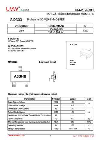
R UMW UMW SI2303 SOT-23 Plastic-Encapsulate MOSFETS P-channel 30-V(D-S) MOSFET SI2303 V(BR)DSS RDS(on)MAX ID 190m @-10V -30 V -1.7A 330m @-4.5V FEATURE TrenchFET Power MOSFET SOT 23 APPLICATION Load Switch for Portable Devices DC/DC Converter 1. GATE MARKING Equivalent Circuit 2. SOURCE 3. DRAIN Maximum ratings ( Ta=25 unless otherwise noted) Parame
as2303.pdf
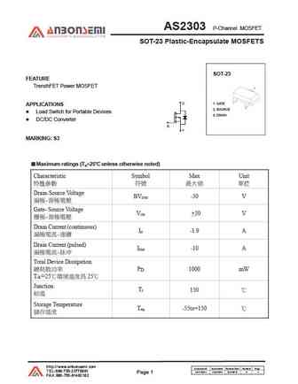
AS2303 P-Channel MOSFET SOT-23 Plastic-Encapsulate MOSFETS Dimensions In Millimeters Dimensions In Inches Symbol Min Max Min Max A 0.900 1.150 0.035 0.045 A1 0.000 0.100 0.000 0.004 A2 0.900 1.050 0.035 0.041 b 0.300 0.500 0.012 0.020 c 0.080 0.150 0.003 0.006 D 2.800 3.000 0.110 0.118 E 1.200 1.400 0.047 0.055 E1 2.250 2.550 0.089 0.100 e 0.9
hoa2303.pdf
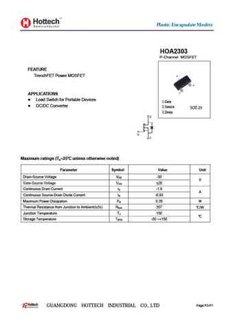
Plastic-Encapsulate Mosfets HOA2303 P-Channel MOSFET FEATURE TrenchFET Power MOSFET APPLICATIONS Load Switch for Portable Devices 1.Gate DC/DC Converter 2.Source SOT-23 3.Drain Maximum ratings (Ta=25 unless otherwise noted) Parameter Symbol Value Unit Drain-Source Voltage VDS -30 V Gate-Source Voltage VGS 20 Continuous Drain Current ID -1.9 A Continuous So
mem2303xg-n.pdf
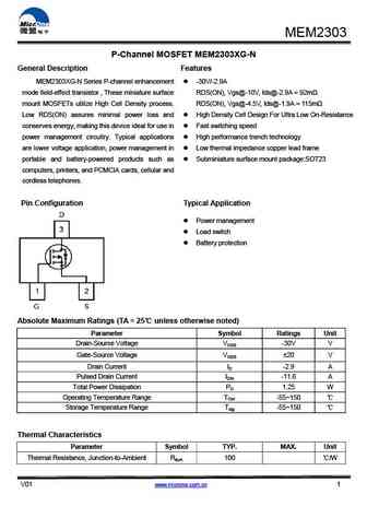
MEM2303 P-Channel MOSFET MEM2303XG-N General Description Features MEM2303XG-N Series P-channel enhancement -30V/-2.9A mode field-effect transistor , These miniature surface RDS(ON), Vgs@-10V, Ids@-2.9A = 92m mount MOSFETs utilize High Cell Density process. RDS(ON), Vgs@-4.5V, Ids@-1.9A = 115m Low RDS(ON) assures minimal power loss and High Density Cell Design For Ultra
mem2303m3.pdf
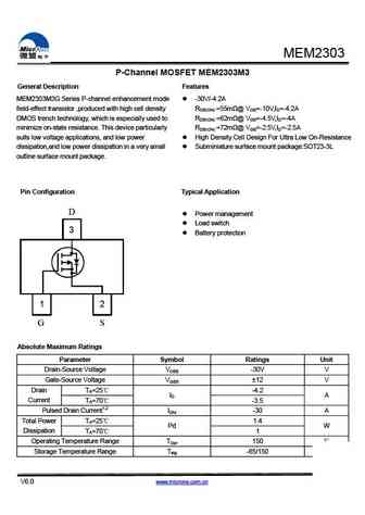
MEM2303 P-Channel MOSFET MEM2303M3 General Description Features MEM2303M3G Series P-channel enhancement mode -30V/-4.2A field-effect transistor ,produced with high cell density RDS(ON) =55m @ VGS=-10V,ID=-4.2A DMOS trench technology, which is especially used to RDS(ON) =62m @ VGS=-4.5V,ID=-4A minimize on-state resistance. This device particularly RDS(ON) =72m @ VGS=-2.5V,ID=-2.5
si2303.pdf
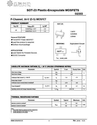
SOT-23 Plastic-Encapsulate MOSFETS SI2303 P-Channel, 30-V (D-S) MOSFET PRODUCT SUMMARY SOT-23 VDS (V) rDS(on) (W) ID (A)b 0.240 @ VGS = 10 V 1.4 30 3 0.460 @ VGS = 4.5 V 1.0 1.GATE 2.SOURCE 3.DRAIN General FEATURE 1 2 TrenchFET Power MOSFET Lead free product is acquired MARKING Equivalent Circuit Surface mount package APPLICATION A96TF w Load Switc
wst2303a.pdf
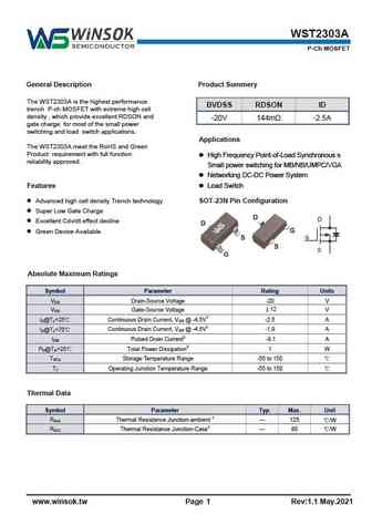
WST2303A P-Ch MOSFET General Description Product Summery The WST2303A is the highest performance BVDSS RDSON ID trench P-ch MOSFET with extreme high cell density , which provide excellent RDSON and -20V 144m -2.5A gate charge for most of the small power switching and load switch applications. Applications The WST2303A meet the RoHS and Green Product requirement with full
wst2303.pdf
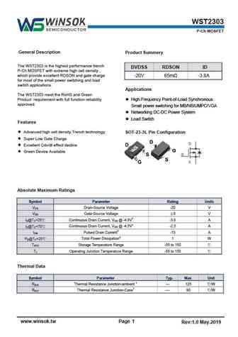
WST2303 P-Ch MOSFET General Description Product Summery The WST2303 is the highest performance trench BVDSS RDSON ID P-Ch MOSFET with extreme high cell density , which provide excellent RDSON and gate charge -20V 65m -3.8A for most of the small power switching and load switch applications. Applications The WST2303 meet the RoHS and Green High Frequency Point-of-Load
apm2303ac.pdf
APM2303AC www.VBsemi.tw P-Channel 30 V (D-S) MOSFET FEATURES PRODUCT SUMMARY TrenchFET Power MOSFET 100 % Rg Tested VDS (V) RDS(on) ( ) Typ. ID (A)a Qg (Typ.) 0.046 at VGS = - 10 V - 5.6 0.049 at VGS = - 6 V - 5 11.4 nC - 30 APPLICATIONS 0.054 at VGS = - 4.5 V -4.5 For Mobile Computing - Load Switch - Notebook Adaptor Switch S TO-236 - DC/DC Converter (SOT-2
yjl2303a.pdf
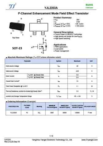
RoHS COMPLIANT YJL2303A P-Channel Enhancement Mode Field Effect Transistor Product Summary V -30V DS I -3.0A D R ( at V =-10V) 85 mohm DS(ON) GS R ( at V =-4.5V) 105 mohm DS(ON) GS General Description Trench Power LV MOSFET technology High density cell design for Low R DS(ON) High Speed switching Applications PMW applicatio
Otros transistores... 2N6796U , 2N6798U , 2N6800LCC4 , 2N6800U , 2N6802U , 2N6845LCC4 , 2N6845U , 2N6847U , NCEP15T14 , 2304 , 2305 , 4414 , 4614 , 4800 , 8958 , 9926 , 045Y .
History: D2N60 | B2N65
🌐 : EN ES РУ

Liste
Recientemente añadidas las descripciónes de los transistores:
MOSFET: AUB034N10 | AUB033N08BG | AUB026N085 | AUA062N08BG | AUA060N08AG | AUA056N08BGL | AUA039N10 | ASW80R290E | ASW65R120EFD | ASW65R110E | ASW65R095EFD | ASW65R046EFD | ASW65R041EFDA | ASW65R041E | ASW60R150E | ASW60R090EFDA
Popular searches
irf640n | 2n3904 | bc547 datasheet | k3797 mosfet | bs170 datasheet | tip41c | irfp460 | irfz44n mosfet