4614 MOSFET Equivalente. Reemplazo. Hoja de especificaciones. Principales características
Número de Parte: 4614
Tipo de FET: MOSFET
Polaridad de transistor: NP
ESPECIFICACIONES MÁXIMAS
Pdⓘ - Máxima
disipación de potencia: 2 W
|Vds|ⓘ - Voltaje máximo drenador-fuente: 40 V
|Vgs|ⓘ - Voltaje máximo fuente-puerta: 20 V
|Id|ⓘ - Corriente continua
de drenaje: 6 A
Tjⓘ - Temperatura máxima de unión: 150 °C
CARACTERÍSTICAS ELÉCTRICAS
trⓘ - Tiempo
de subida: 3.3 nS
Cossⓘ - Capacitancia de salida: 95 pF
RDSonⓘ - Resistencia estado encendido drenaje a fuente: 0.031 Ohm
Encapsulados: SOP-8
Búsqueda de reemplazo de 4614 MOSFET
- Selecciónⓘ de transistores por parámetros
4614 datasheet
..1. Size:433K sztuofeng
4614.pdf 
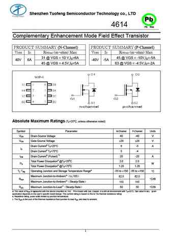
Shenzhen Tuofeng Semiconductor Technology co., LTD Pb 4614 Pb free Complementary Enhancement Mode Field Effect Transistor PRODUCT SUMMARY (N-Channel) PRODUCT SUMMARY (P-Channel) VDSS ID RDS(on) (m-ohm) Max VDSS ID RDS(on) (m-ohm) Max 31 @ VGS = 10 V,ID=6A 45 @ VGS = -10V,ID=-5A 40V 6A -40V -5A 45 @ VGS = 4.5V,ID=5A 63 @ VGS = -4.5V,ID=-2A Absolute Maximum Ratings (T =25oC, un
0.1. Size:137K sanyo
2sc4614.pdf
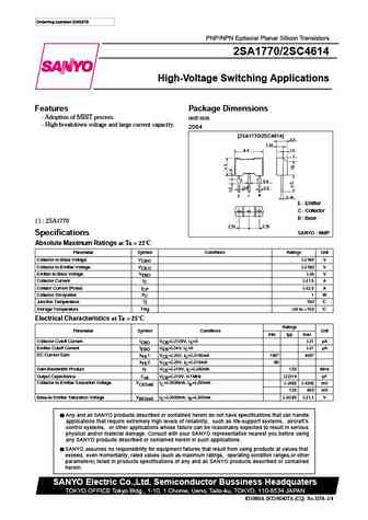
Ordering number EN3578 PNP/NPN Epitaxial Planar Silicon Transistors 2SA1770/2SC4614 High-Voltage Switching Applications Features Package Dimensions Adoption of MBIT process. unit mm High breakdown voltage and large current capacity. 2064 [2SA1770/2SC4614] E Emitter C Collector B Base ( ) 2SA1770 SANYO NMP Specifications Absolute Maximum Ratings at Ta = 25 C P
0.2. Size:60K sanyo
2sa1770 2sc4614.pdf
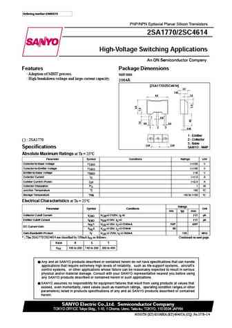
Ordering number ENN3578 PNP/NPN Epitaxial Planar Silicon Transistors 2SA1770/2SC4614 High-Voltage Switching Applications Features Package Dimensions Adoption of MBIT process. unit mm High breakdown voltage and large current capacity. 2064A [2SA1770/2SC4614] 2.5 1.45 6.9 1.0 0.6 0.9 0.5 1 2 3 0.45 1 Emitter 2 Collector ( ) 2SA1770 3 Base 2.54 2.54 Specificat
0.3. Size:541K onsemi
2sa1770s-an 2sa1770t-an 2sc4614s-an 2sc4614t-an.pdf
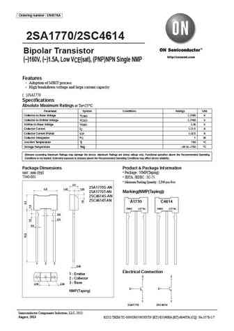
Ordering number EN3578A 2SA1770/2SC4614 Bipolar Transistor http //onsemi.com ( ) ( ) ( ) ( ) 160V, 1.5A, Low VCE sat , PNP NPN Single NMP Features Adoption of MBIT process High breakdown voltage and large current capacity ( )2SA1770 Specifications Absolute Maximum Ratings at Ta=25 C Parameter Symbol Conditions Ratings Unit Collector-to-Base Voltage VCBO (--)180 V C
0.4. Size:217K aosemi
ao4614.pdf
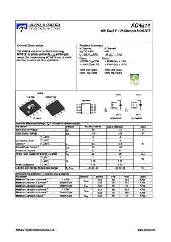
AO4614 40V Dual P + N-Channel MOSFET General Description Product Summary N-Channel P-Channel The AO4614 uses advanced trench technology VDS (V) = 40V -40V MOSFETs to provide excellent RDS(ON) and low gate ID = 6A (VGS=10V) -5A (VGS = -10V) charge. The complementary MOSFETs may be used in RDS(ON) RDS(ON) H-bridge, Inverters and other applications.
0.5. Size:233K aosemi
ao4614b.pdf
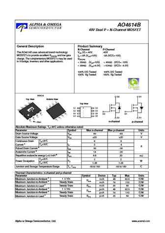
AO4614B 40V Dual P + N-Channel MOSFET General Description Product Summary N-Channel P-Channel The AO4614B uses advanced trench technology VDS (V) = 40V, -40V MOSFETs to provide excellent RDS(ON) and low gate ID = 6A (VGS=10V) -5A (VGS=-10V) charge. The complementary MOSFETs may be used RDS(ON) in H-bridge, Inverters and other applications.
0.6. Size:1103K blue-rocket-elect
brcs4614sc.pdf
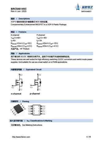
BRCS4614SC Rev.A Jun.-2020 DATA SHEET / Descriptions SOP-8 MOS Complementary Enhancement MOSFET in a SOP-8 Plastic Package. / Features N-channel P-channel VDS(V)=40V VDS(V)=-40V ID=6A ID=-5A RDS(ON)
0.7. Size:1597K kexin
ao4614b.pdf
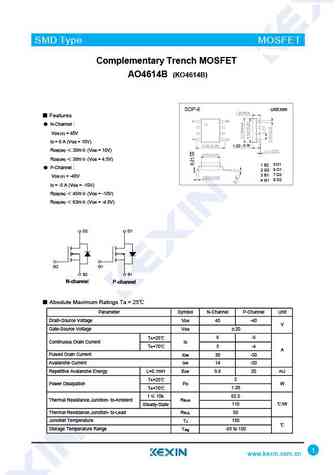
SMD Type MOSFET Complementary Trench MOSFET AO4614B (KO4614B) SOP-8 Unit mm Features N-Channel VDS (V) = 40V ID = 6 A (VGS = 10V) 1.50 0.15 RDS(ON) 30m (VGS = 10V) RDS(ON) 38m (VGS = 4.5V) 1 S2 5 D1 P-Channel 6 D1 2 G2 7 D2 3 S1 VDS (V) = -40V 8 D2 4 G1 ID = -5 A (VGS = -10V) RDS(ON) 45m (VGS = -10V) RDS(ON) 63m (VGS = -4.5V)
0.8. Size:2230K kexin
ao4614a.pdf
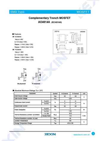
SMD Type MOSFET Complementary Trench MOSFET AO4614A (KO4614A) SOP-8 Unit mm Features N-Channel VDS (V) = 40V ID = 6 A (VGS = 10V) 1.50 0.15 RDS(ON) 31m (VGS = 10V) RDS(ON) 45m (VGS = 4.5V) 1 S2 5 D1 6 D1 P-Channel 2 G2 7 D2 3 S1 VDS (V) = -40V 8 D2 4 G1 ID = -5 A (VGS = -10V) RDS(ON) 45m (VGS = -10V) RDS(ON) 63m (VGS = -4.5V)
0.9. Size:624K elm
elm14614aa.pdf
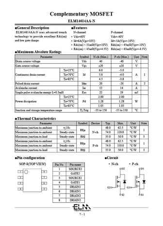
Complementary MOSFET ELM14614AA-N General Description Features ELM14614AA-N uses advanced trench N-channel P-channel technology to provide excellent Rds(on) Vds=40V Vds=-40V and low gate charge. Id=6A(Vgs=10V) Id=-5A(Vgs=-10V) Rds(on)
0.10. Size:1021K ncepower
nce4614b.pdf
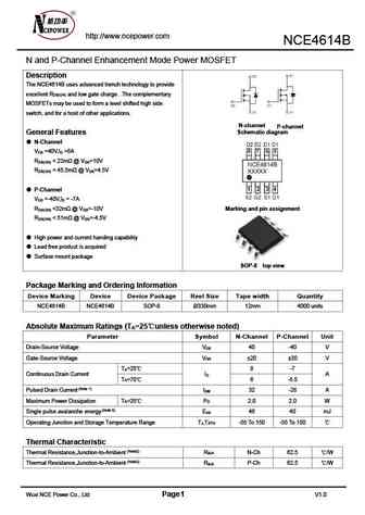
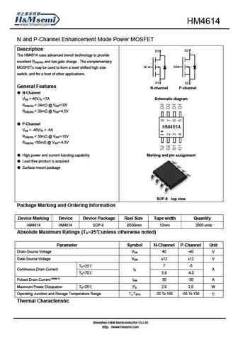
http //www.ncepower.com NCE4614B N and P-Channel Enhancement Mode Power MOSFET Description The NCE4614B uses advanced trench technology to provide excellent R and low gate charge . The complementary DS(ON) MOSFETs may be used to form a level shifted high side switch, and for a host of other applications. N-channel P-channel Schematic diagram General Features N-Channel V =40V,I
0.11. Size:531K ncepower
nce4614.pdf
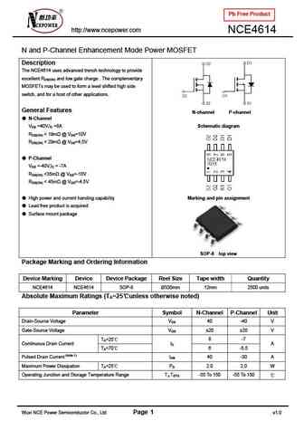
Pb Free Product http //www.ncepower.com NCE4614 N and P-Channel Enhancement Mode Power MOSFET Description The NCE4614 uses advanced trench technology to provide excellent RDS(ON) and low gate charge . The complementary MOSFETs may be used to form a level shifted high side switch, and for a host of other applications. General Features N-channel P-channel N-Channel VDS =4
0.12. Size:1011K ncepower
nce4614c.pdf
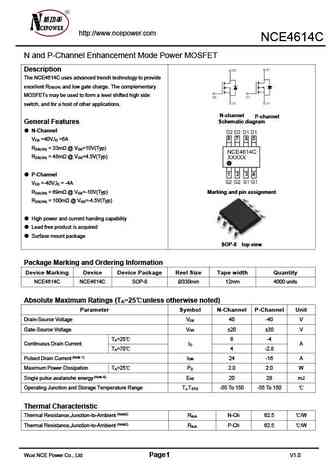
http //www.ncepower.com NCE4614C N and P-Channel Enhancement Mode Power MOSFET Description The NCE4614C uses advanced trench technology to provide excellent R and low gate charge. The complementary DS(ON) MOSFETs may be used to form a level shifted high side switch, and for a host of other applications. N-channel P-channel Schematic diagram General Features N-Channel V =40V,I
0.13. Size:9489K slkor
sl4614.pdf
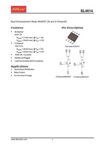
SL4614 Dual Enhancement Mode MOSFET (N-and P-Channel) Features Pin Description D1 N Channel D1 D2 D2 40V/7.5A, RDS(ON) = 21m (max.) @ VGS = 10V S1 RDS(ON) = 25m (max.) @ VGS = 4.5V G1 S2 P Channel G2 -40V/-5.5A, Top View of SOP-8 RDS(ON) = 38m (max.) @ VGS =-10V (8) (7) (6) (5) D1 D1 RDS(ON) = 62m (max.) @ VGS =-4.5V D2 D2 100% UIS + Rg Tested Reliable and Rugged
0.14. Size:1529K stansontech
stc4614.pdf
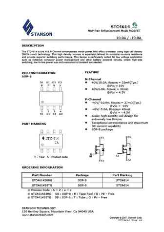
STC4614 N&P Pair Enhancement Mode MOSFET 10.0A / -10.0A DESCRIPTION The STC4614 is the N & P-Channel enhancement mode power field effect transistor using high cell density DMOS trench technology. This high density process is especially tailored to minimize on-state resistance and provide superior switching performance. This device is particularly suited for low voltage application
0.15. Size:464K ascend
asdm4614s.pdf
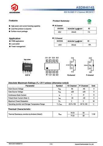
ASDM4614S 40V N A ND P-Channel MOSFET Features Product Summary N-Channel High power and current handing capability BVDSS ID Lead free product is acquired RDSON.Typ@10V Surface mount package 40V 28m 7A P-Channel Application PWM applications BVDSS ID RDSON.Typ@10V Load switch -6A -40V 38m Power management top view ASCEND N-channel P-ch
0.16. Size:3951K cn szxunrui
si4614.pdf
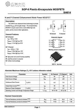
SOP-8 Plastic-Encapsulate MOSFETS SI4614 N and P-Channel Enhancement Mode Power MOSFET Description The SI4614 uses advanced trench technology to provide excellent RDS(ON) and low gate charge . The complementary MOSFETs may be used to form a level shifted high side switch, and for a host of other applications. N-channel P-channel General Features N-Channel Schematic diagr
0.17. Size:558K cn puolop
pts4614.pdf
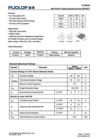
PTS4614 40V/7A N+P Channel Advanced Power MOSFET Features Low RDS(on) @VGS=5V Key Items NMOS PMOS Unit 5V Logic Level Control BVDSS 40 -40 V N+P Dual Channel SOP8 Package ID 8 7 A Pb-Free, RoHS Compliant RDSON1 14 28 m RDSON2 19 33 m Applications High Side Load Switch Battery Switch Optimized for Power Management Applications for Po
0.18. Size:1608K cn twgmc
tw4614sq-x.pdf
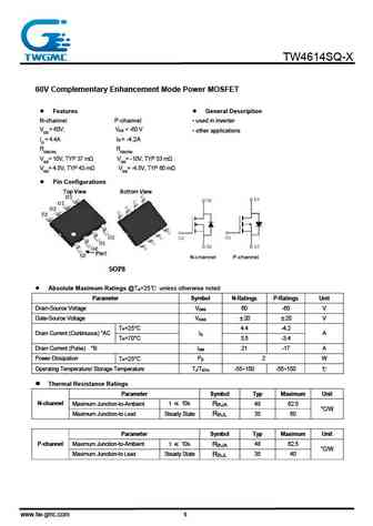
TW4614SQ-X 60V Complementary Enhancement Mode Power MOSFET Features General Description N-channel P-channel used in inverter VDS = 60V, VDS = -60 V other applications ID = 4.4A ID = -4.2A RDS(ON) RDS(ON) VGS= 10V, TYP 37 m VGS= -10V, TYP 53 m VGS= 4.5V, TYP 43 m VGS= -4.5V, TYP 60 m Pin Configurations SOP8 Absolute Maximum Ratings @T =25
0.19. Size:795K cn sps
sm4614bprl.pdf
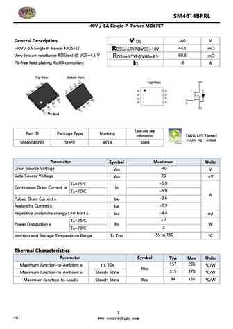
SM4614BPRL -40V /-6A Single P Power MOSFET C P04C P -40V /-6A Single P Power MOSFET 6P04C General Description -40 V V DS -40V /-6A Single P Power MOSFET 44.1 m RDS(on),TYP@VGS=10V Very low on-resistance RDS(on) @ VGS=4.5 V 69.3 m RDS(on),TYP@VGS=4.5 Pb-free lead plating; RoHS compliant -6 A ID Tape and reel Part ID Package Type Marking infomation 100% UIS Tested 100% Rg Test
0.20. Size:891K cn vbsemi
ao4614-30v.pdf
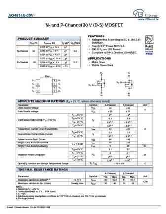
AO4614&-30V www.VBsemi.tw N- and P-Channel 30 V (D-S) MOSFET FEATURES PRODUCT SUMMARY Halogen-free According to IEC 61249-2-21 VDS (V) RDS(on) ( ) Definition ID (A)a Qg (Typ.) TrenchFET Power MOSFET 0.018 at VGS = 10 V 8e 100 % Rg and UIS Tested N-Channel 30 0.020 at VGS = 8 V 8e 6.2 Compliant to RoHS Directive 2002/95/EC 0.024 at VGS = 4.5 V 8e 0.032 at
0.22. Size:1361K cn hmsemi
hm4614b.pdf
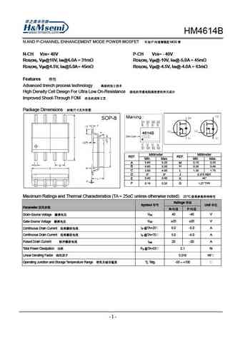
HM N AND P-CHANNEL ENHANCEMENT MODE POWER MOSFET N P MOS N-CH VDS= 40V P-CH VDS= - 40V RDS(ON), Vgs@10V, Ids@6.0A = 31m RDS(ON), Vgs@-10V, Ids@-5.0A = 45m RDS(ON), Vgs@4.5V, Ids@5.0A= 45m RDS(ON), Vgs@-4.5V, Ids@-4.0A = 63m Features Advanced trench process technology High Density Cell Design For Ultra Low On-Resist
0.23. Size:1010K cn vgsemi
vs4614as-a.pdf
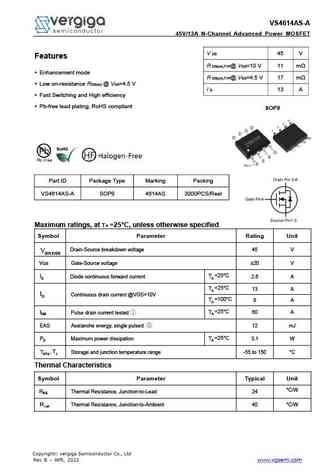
VS4614AS-A 45V/13A N-Channel Advanced Power MOSFET V DS 45 V Features R DS(on),TYP@ VGS=10 V 11 m Enhancement mode R DS(on),TYP@ VGS=4.5 V 17 m Low on-resistance RDS(on) @ VGS=4.5 V I D 13 A Fast Switching and High efficiency Pb-free lead plating; RoHS compliant SOP8 Part ID Package Type Marking Packing VS4614AS-A SOP8 4614AS 3000PCS/Reel Maximum ratings, at
Otros transistores... 2N6802U
, 2N6845LCC4
, 2N6845U
, 2N6847U
, 2303
, 2304
, 2305
, 4414
, TK10A60D
, 4800
, 8958
, 9926
, 045Y
, 06N03
, 10N60A
, 10N60AF
, 10N60H
.