13N60AF MOSFET Equivalente. Reemplazo. Hoja de especificaciones. Principales características
Número de Parte: 13N60AF
Tipo de FET: MOSFET
Polaridad de transistor: N
ESPECIFICACIONES MÁXIMAS
Pdⓘ - Máxima
disipación de potencia: 34 W
|Vds|ⓘ - Voltaje máximo drenador-fuente: 600 V
|Vgs|ⓘ - Voltaje máximo fuente-puerta: 30 V
|Id|ⓘ - Corriente continua
de drenaje: 13 A
Tjⓘ - Temperatura máxima de unión: 150 °C
CARACTERÍSTICAS ELÉCTRICAS
trⓘ - Tiempo
de subida: 10.5 nS
Cossⓘ - Capacitancia de salida: 50 pF
RDSonⓘ - Resistencia estado encendido drenaje a fuente: 0.26 Ohm
Encapsulados: TO-220F
Búsqueda de reemplazo de 13N60AF MOSFET
- Selecciónⓘ de transistores por parámetros
13N60AF datasheet
..1. Size:366K nell
13n60a 13n60af.pdf 
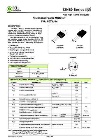
RoHS 13N60 Series RoHS SEMICONDUCTOR Nell High Power Products N-Channel Power MOSFET 13A, 600Volts DESCRIPTION The Nell 13N60 is a three-terminal silicon device with current conduction capability of D 13A, fast switching speed, low on-state resistance, breakdown voltage rating of 600V, and max. threshold voltage of 4 volts. They are designed for use in applications such as s
9.1. Size:643K 1
sgs13n60ufd.pdf
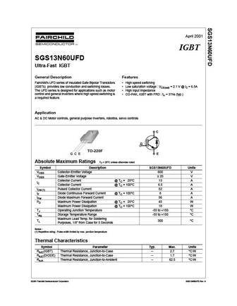
April 2001 IGBT SGS13N60UFD Ultra-Fast IGBT General Description Features Fairchild's UFD series of Insulated Gate Bipolar Transistors High speed switching (IGBTs) provides low conduction and switching losses. Low saturation voltage VCE(sat) = 2.1 V @ IC = 6.5A The UFD series is designed for applications such as motor High input impedance control and general inverters whe
9.2. Size:584K 1
sgs13n60uf.pdf
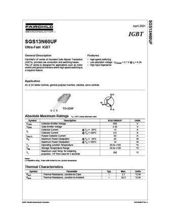
April 2001 IGBT SGS13N60UF Ultra-Fast IGBT General Description Features Fairchild's UF series of Insulated Gate Bipolar Transistors High speed switching (IGBTs) provides low conduction and switching losses. Low saturation voltage VCE(sat) = 2.1 V @ IC = 6.5A The UF series is designed for applications such as motor High input impedance control and general inverters where
9.3. Size:1324K 1
pfp13n60 pff13n60.pdf
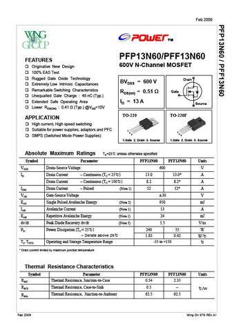
Feb 2009 PFP13N60/PFF13N60 FEATURES 600V N-Channel MOSFET Originative New Design 100% EAS Test Rugged Gate Oxide Technology Drain BVDSS = 600 V Extremely Low Intrinsic Capacitances Remarkable Switching Characteristics Gate RDS(on) = 0.51 Unequalled Gate Charge 48 nC (Typ.)
9.4. Size:1047K st
stl13n60m2.pdf
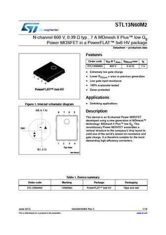
STL13N60M2 N-channel 600 V, 0.39 typ., 7 A MDmesh II Plus low Qg Power MOSFET in a PowerFLAT 5x6 HV package Datasheet - production data Features Order code VDS @ TJmax RDS(on) max ID STL13N60M2 650 V 0.42 7 A Extremely low gate charge Lower RDS(on) x area vs previous generation 1 2 3 Low gate input resistance 4 100% avalanche tested PowerFLAT 5x6
9.5. Size:1515K st
stb13n60m2 std13n60m2.pdf
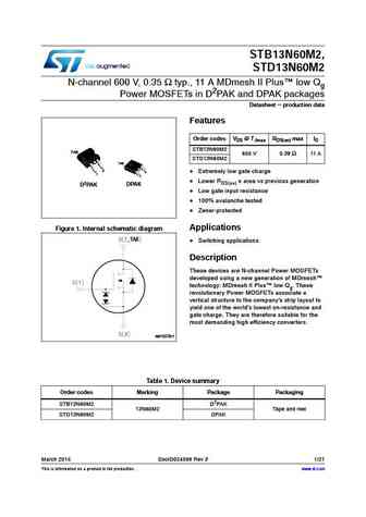
STB13N60M2, STD13N60M2 N-channel 600 V, 0.35 typ., 11 A MDmesh II Plus low Qg Power MOSFETs in D2PAK and DPAK packages Datasheet - production data Features Order codes VDS @ TJmax RDS(on) max ID STB13N60M2 TAB 650 V 0.38 11 A STD13N60M2 TAB 3 3 Extremely low gate charge 1 1 Lower RDS(on) x area vs previous generation DPAK D2PAK Low gate input resistance
9.6. Size:1256K st
stp13n60m2 stu13n60m2 stw13n60m2.pdf
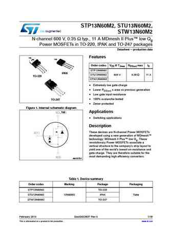
STP13N60M2, STU13N60M2, STW13N60M2 N-channel 600 V, 0.35 typ., 11 A MDmesh II Plus low Qg Power MOSFETs in TO-220, IPAK and TO-247 packages Datasheet - production data Features TAB TAB Order codes VDS @ TJmax RDS(on) max ID 3 2 1 STP13N60M2 3 2 1 IPAK STU13N60M2 650 V 0.38 11 A TO-220 STW13N60M2 Extremely low gate charge Lower RDS(on) x area vs previous g
9.7. Size:1131K st
stf13n60m2 stfi13n60m2.pdf
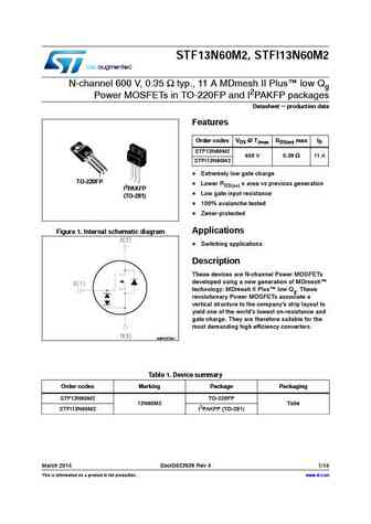
STF13N60M2, STFI13N60M2 N-channel 600 V, 0.35 typ., 11 A MDmesh II Plus low Qg Power MOSFETs in TO-220FP and I2PAKFP packages Datasheet - production data Features Order codes VDS @ TJmax RDS(on) max ID STF13N60M2 650 V 0.38 11 A STFI13N60M2 3 2 Extremely low gate charge 1 1 2 3 TO-220FP Lower RDS(on) x area vs previous generation I2PAKFP Low gate input r
9.8. Size:443K st
stf13n60dm2.pdf

STF13N60DM2 Datasheet N-channel 600 V, 0.310 typ., 11 A MDmesh DM2 Power MOSFET in a TO-220FP package VDS RDS(on) max. ID Order codes STF13N60DM2 600 V 0.365 11 A Fast-recovery body diode Extremely low gate charge and input capacitance Low on-resistance 3 2 1 100% avalanche tested Extremely high dv/dt ruggedness TO-220FP Zener-protected D(2) A
9.9. Size:513K st
std13n60dm2.pdf
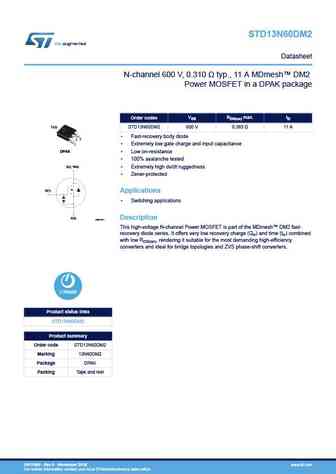
STD13N60DM2 Datasheet N-channel 600 V, 0.310 typ., 11 A MDmesh DM2 Power MOSFET in a DPAK package VDS RDS(on) max. ID Order codes TAB STD13N60DM2 600 V 0.365 11 A Fast-recovery body diode 3 2 1 Extremely low gate charge and input capacitance DPAK Low on-resistance 100% avalanche tested D(2, TAB) Extremely high dv/dt ruggedness Zener-protected
9.10. Size:451K st
stp13n60dm2.pdf
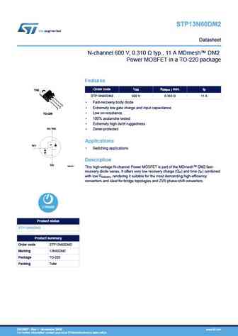
STP13N60DM2 Datasheet N-channel 600 V, 0.310 typ., 11 A MDmesh DM2 Power MOSFET in a TO-220 package Features VDS RDS(on ) max. ID Order code TAB STP13N60DM2 600 V 0.365 11 A Fast-recovery body diode 3 2 Extremely low gate charge and input capacitance 1 Low on-resistance TO-220 100% avalanche tested Extremely high dv/dt ruggedness D(2, TAB) Ze
9.11. Size:898K fairchild semi
fcp13n60n fcpf13n60nt.pdf
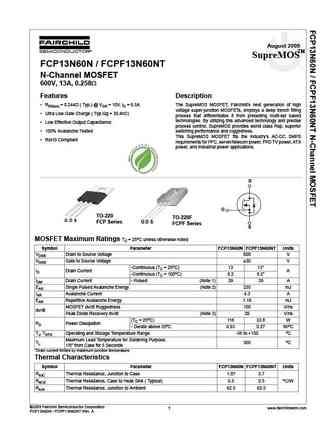
August 2009 SupreMOSTM FCP13N60N / FCPF13N60NT N-Channel MOSFET 600V, 13A, 0.258 Features Description RDS(on) = 0.244 ( Typ.) @ VGS = 10V, ID = 6.5A The SupreMOS MOSFET, Fairchild s next generation of high voltage super-junction MOSFETs, employs a deep trench filling Ultra Low Gate Charge ( Typ.Qg = 30.4nC) process that differentiates it from preceding multi-epi based
9.12. Size:537K fairchild semi
sgp13n60uf.pdf
IGBT SGP13N60UF Ultra-Fast IGBT General Description Features Fairchild's UF series of Insulated Gate Bipolar Transistors High speed switching (IGBTs) provides low conduction and switching losses. Low saturation voltage VCE(sat) = 2.1 V @ IC = 6.5A The UF series is designed for applications such as motor High input impedance control and general inverters where high speed s
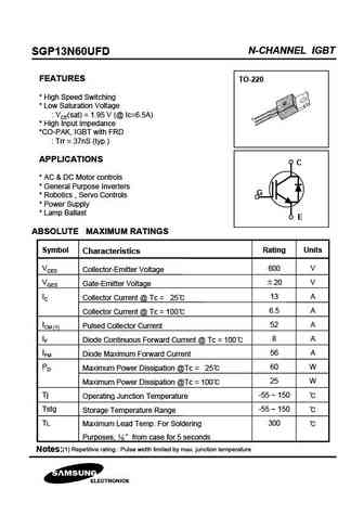
9.13. Size:615K fairchild semi
sgp13n60ufd.pdf
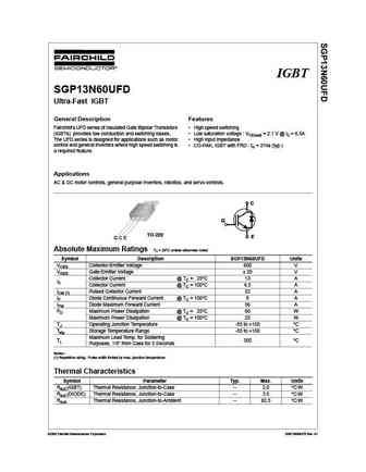
IGBT SGP13N60UFD Ultra-Fast IGBT General Description Features Fairchild's UFD series of Insulated Gate Bipolar Transistors High speed switching (IGBTs) provides low conduction and switching losses. Low saturation voltage VCE(sat) = 2.1 V @ IC = 6.5A The UFD series is designed for applications such as motor High input impedance control and general inverters where high spee
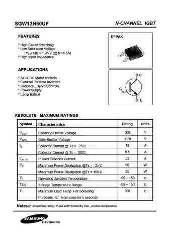
9.14. Size:274K samsung
sgw13n60ufd.pdf
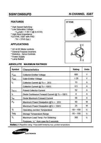
N-CHANNEL IGBT SGW13N60UFD FEATURES D2-PAK * High Speed Switching * Low Saturation Voltage VCE(sat) = 1.95 V (@ Ic=6.5A) * High Input Impedance *CO-PAK, IGBT with FRD Trr = 37nS (typ.) APPLICATIONS C * AC & DC Motor controls * General Purpose Inverters G * Robotics , Servo Controls * Power Supply * Lamp Ballast E ABSOLUTE MAXIMUM RATINGS Symbol Rating Units Charac
9.15. Size:274K samsung
sgh13n60ufd.pdf
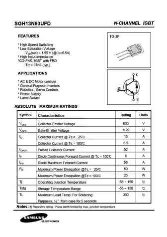
N-CHANNEL IGBT SGH13N60UFD FEATURES TO-3P * High Speed Switching * Low Saturation Voltage VCE(sat) = 1.95 V (@ Ic=6.5A) * High Input Impedance *CO-PAK, IGBT with FRD Trr = 37nS (typ.) APPLICATIONS C * AC & DC Motor controls * General Purpose Inverters G * Robotics , Servo Controls * Power Supply * Lamp Ballast E ABSOLUTE MAXIMUM RATINGS Symbol Rating Units Charact
9.16. Size:230K samsung
sgp13n60uf.pdf
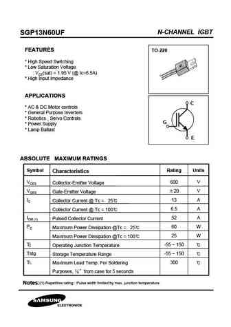
N-CHANNEL IGBT SGP13N60UF FEATURES TO-220 * High Speed Switching * Low Saturation Voltage VCE(sat) = 1.95 V (@ Ic=6.5A) * High Input Impedance APPLICATIONS C * AC & DC Motor controls * General Purpose Inverters * Robotics , Servo Controls G * Power Supply * Lamp Ballast E ABSOLUTE MAXIMUM RATINGS Symbol Rating Units Characteristics VCES 600 V Collector-Emitter Voltage
9.17. Size:274K samsung
sgp13n60ufd.pdf
N-CHANNEL IGBT SGP13N60UFD FEATURES TO-220 * High Speed Switching * Low Saturation Voltage VCE(sat) = 1.95 V (@ Ic=6.5A) * High Input Impedance *CO-PAK, IGBT with FRD Trr = 37nS (typ.) APPLICATIONS C * AC & DC Motor controls * General Purpose Inverters G * Robotics , Servo Controls * Power Supply * Lamp Ballast E ABSOLUTE MAXIMUM RATINGS Symbol Rating Units Charac
9.18. Size:230K samsung
sgw13n60uf.pdf
N-CHANNEL IGBT SGW13N60UF FEATURES D2-PAK * High Speed Switching * Low Saturation Voltage VCE(sat) = 1.95 V (@ Ic=6.5A) * High Input Impedance APPLICATIONS C * AC & DC Motor controls * General Purpose Inverters * Robotics , Servo Controls G * Power Supply * Lamp Ballast E ABSOLUTE MAXIMUM RATINGS Symbol Rating Units Characteristics VCES 600 V Collector-Emitter Voltage
9.19. Size:100K ixys
ixkp13n60c5m.pdf
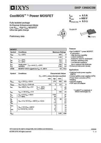
IXKP 13N60C5M ID25 = 6.5 A CoolMOS 1) Power MOSFET VDSS = 600 V RDS(on) max = 0.3 Fully isolated package N-Channel Enhancement Mode Low RDSon, High VDSS MOSFET D TO-220 FP Ultra low gate charge G D G S Preliminary data S Features MOSFET fast CoolMOS 1) power MOSFET Symbol Conditions Maximum Ratings 4th generation VDSS TVJ = 25 C 600 V - High blocking capabi
9.20. Size:785K onsemi
fcp13n60n fcpf13n60nt.pdf

Is Now Part of To learn more about ON Semiconductor, please visit our website at www.onsemi.com Please note As part of the Fairchild Semiconductor integration, some of the Fairchild orderable part numbers will need to change in order to meet ON Semiconductor s system requirements. Since the ON Semiconductor product management systems do not have the ability to manage part nomenclatur
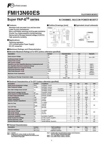
9.21. Size:529K fuji
fmv13n60es.pdf
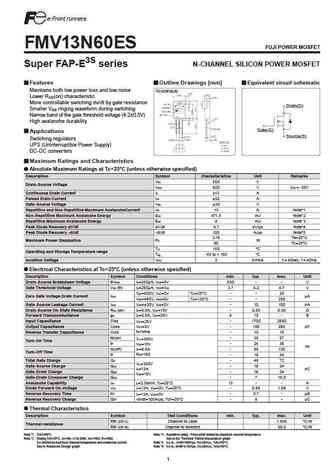
FMV13N60ES FUJI POWER MOSFET Super FAP-E3S series N-CHANNEL SILICON POWER MOSFET Features Outline Drawings [mm] Equivalent circuit schematic Maintains both low power loss and low noise TO-220F(SLS) Lower R (on) characteristic DS More controllable switching dv/dt by gate resistance Drain(D) Smaller V ringing waveform during switching GS Narrow band of the gate threshold voltage (4.2
9.22. Size:536K fuji
fmc13n60es.pdf

FMC13N60ES FUJI POWER MOSFET Super FAP-E3S series N-CHANNEL SILICON POWER MOSFET Features Outline Drawings [mm] Equivalent circuit schematic Maintains both low power loss and low noise T-Pack(S) Lower R (on) characteristic DS More controllable switching dv/dt by gate resistance Drain(D) Smaller V ringing waveform during switching GS Narrow band of the gate threshold voltage (4.2 0.5
9.23. Size:471K fuji
fmc13n60e.pdf
FMC13N60E FUJI POWER MOSFET Super FAP-E3 series N-CHANNEL SILICON POWER MOSFET Features Outline Drawings [mm] Equivalent circuit schematic Maintains both low power loss and low noise T-Pack(S) Lower R (on) characteristic DS More controllable switching dv/dt by gate resistance Drain(D) Smaller V ringing waveform during switching GS Narrow band of the gate threshold voltage (3.0 0.5V)
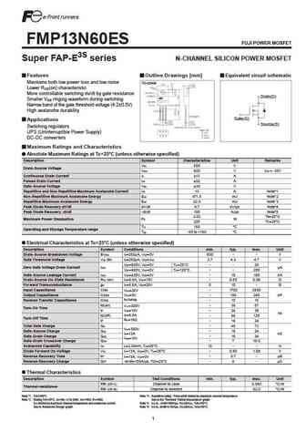
9.24. Size:540K fuji
fmh13n60es.pdf
FMH13N60ES FUJI POWER MOSFET Super FAP-E3S series N-CHANNEL SILICON POWER MOSFET Features Outline Drawings [mm] Equivalent circuit schematic Maintains both low power loss and low noise TO-3P(Q) Lower R (on) characteristic DS More controllable switching dv/dt by gate resistance Drain(D) Smaller V ringing waveform during switching GS Narrow band of the gate threshold voltage (4.2 0.5V
9.25. Size:466K fuji
fmv13n60e.pdf
FMV13N60E FUJI POWER MOSFET Super FAP-E3 series N-CHANNEL SILICON POWER MOSFET Features Outline Drawings [mm] Equivalent circuit schematic Maintains both low power loss and low noise TO-220F(SLS) Lower R (on) characteristic DS More controllable switching dv/dt by gate resistance Drain(D) Smaller V ringing waveform during switching GS Narrow band of the gate threshold voltage (3.0 0.
9.26. Size:471K fuji
fmi13n60e.pdf
FMI13N60E FUJI POWER MOSFET Super FAP-E3 series N-CHANNEL SILICON POWER MOSFET Features Outline Drawings [mm] Equivalent circuit schematic Maintains both low power loss and low noise T-Pack(L) Lower R (on) characteristic DS More controllable switching dv/dt by gate resistance Drain(D) Smaller V ringing waveform during switching GS Narrow band of the gate threshold voltage (3.0 0.5V)
9.27. Size:536K fuji
fmi13n60es.pdf
FMI13N60ES FUJI POWER MOSFET Super FAP-E3S series N-CHANNEL SILICON POWER MOSFET Features Outline Drawings [mm] Equivalent circuit schematic Maintains both low power loss and low noise T-Pack(L) Lower R (on) characteristic DS More controllable switching dv/dt by gate resistance Drain(D) Smaller V ringing waveform during switching GS Narrow band of the gate threshold voltage (
9.28. Size:466K fuji
fmp13n60e.pdf

FMP13N60E FUJI POWER MOSFET Super FAP-E3 series N-CHANNEL SILICON POWER MOSFET Features Outline Drawings [mm] Equivalent circuit schematic Maintains both low power loss and low noise TO-220AB Lower R (on) characteristic DS More controllable switching dv/dt by gate resistance Drain(D) Smaller V ringing waveform during switching GS Narrow band of the gate threshold voltage (3.0 0.5V)
9.29. Size:528K fuji
fmp13n60es.pdf
FMP13N60ES FUJI POWER MOSFET Super FAP-E3S series N-CHANNEL SILICON POWER MOSFET Features Outline Drawings [mm] Equivalent circuit schematic Maintains both low power loss and low noise TO-220AB Lower R (on) characteristic DS More controllable switching dv/dt by gate resistance Drain(D) Smaller V ringing waveform during switching GS Narrow band of the gate threshold voltage (4.2 0.5
9.30. Size:310K fuji
fml13n60es.pdf
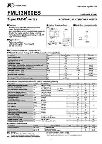
http //www.fujisemi.com FML13N60ES FUJI POWER MOSFET Super FAP-E3 series N-CHANNEL SILICON POWER MOSFET Features Outline Drawings [mm] Equivalent circuit schematic Maintains both low power loss and low noise TFP 9.0 0.2 7.0 0.2 0.4 0.1 Lower R (on) characteristic DS 4 More controllable switching dv/dt by gate resistance 4 D Smaller V ringing waveform during switching GS Narrow
9.31. Size:65K kec
kf13n60n.pdf
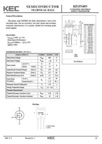
KF13N60N SEMICONDUCTOR N CHANNEL MOS FIELD TECHNICAL DATA EFFECT TRANSISTOR General Description A This planar stripe MOSFET has better characteristics, such as fast Q B N O K switching time, low on resistance, low gate charge and excellent DIM MILLIMETERS avalanche characteristics. It is mainly suitable for switching mode _ A + 15.60 0.20 _ B 4.80 + 0.20 power supplies. _
9.32. Size:507K jiaensemi
jfpc13n60ci.pdf
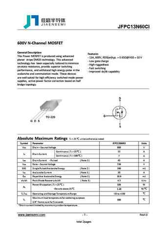
JFPC13N60CI 600V N-Channel MOSFET General Description Features This Power MOSFET is produced using advanced - 13A, 600V, RDS(on)typ. = 0.65 @VGS = 10 V planar stripe DMOS technology. This advanced - Low gate charge technology has been especially tailored to minimize - High ruggedness on-state resistance, provide superior switching - Fast switching performance, and withs
9.33. Size:837K pipsemi
ptp13n60 pta13n60.pdf
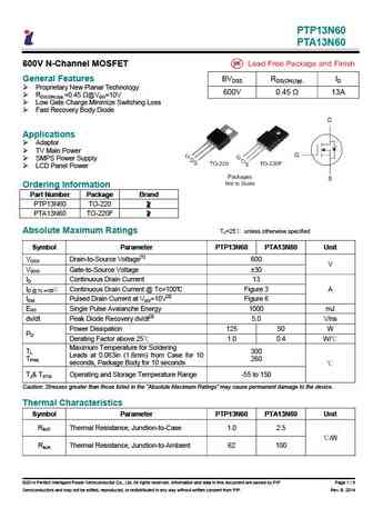
PTP13N60 PTA13N60 600V N-Channel MOSFET General Features BVDSS RDS(ON),typ. ID Proprietary New Planar Technology 600V 0.45 13A RDS(ON),typ.=0.45 @VGS=10V Low Gate Charge Minimize Switching Loss Fast Recovery Body Diode Applications Adaptor TV Main Power SMPS Power Supply LCD Panel Power Ordering Information Part Number Package Brand PTP13N60 TO-22
9.34. Size:596K samwin
swf13n60d.pdf
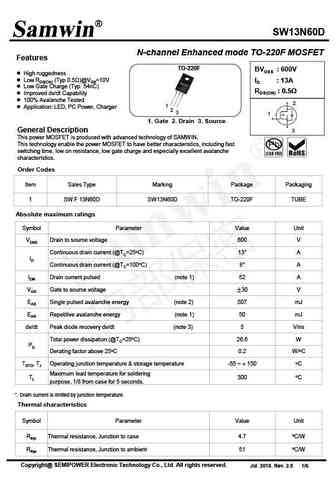
SW13N60D N-channel Enhanced mode TO-220F MOSFET Features TO-220F BVDSS 600V High ruggedness Low RDS(ON) (Typ 0.5 )@VGS=10V ID 13A Low Gate Charge (Typ 54nC) RDS(ON) 0.5 Improved dv/dt Capability 100% Avalanche Tested 2 1 Application LED, PC Power, Charger 2 3 1 1. Gate 2. Drain 3. Source General Description 3 This pow
9.35. Size:878K samwin
swf13n60k2 swi13n60k2 swd13n60k2.pdf
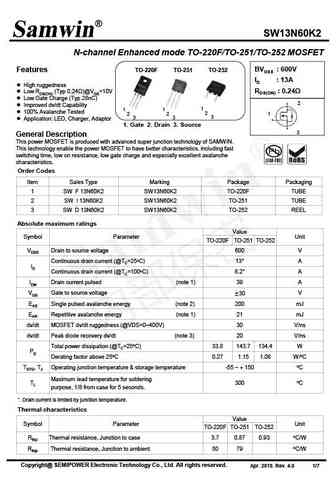
SW13N60K2 N-channel Enhanced mode TO-220F/TO-251/TO-252 MOSFET BVDSS 600V Features TO-220F TO-251 TO-252 ID 13A High ruggedness RDS(ON) 0.24 Low RDS(ON) (Typ 0.24 )@VGS=10V Low Gate Charge (Typ 28nC) 2 Improved dv/dt Capability 1 1 1 100% Avalanche Tested 2 2 2 1 3 3 3 Application LED, Charger, Adaptor 1. Gate 2. Drain 3
9.36. Size:185K semihow
hfs13n60u.pdf
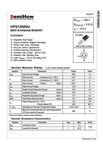
Sep 2012 BVDSS = 600 V RDS(on) typ = 0.33 HFS13N60U ID = 14.0 A 600V N-Channel MOSFET TO-220F FEATURES Originative New Design Superior Avalanche Rugged Technology 1 2 3 Robust Gate Oxide Technology 1.Gate 2. Drain 3. Source Very Low Intrinsic Capacitances Excellent Switching Characteristics Unrivalled Gate Charge 60.0 nC (Typ.) Extended Safe Operating Area
9.37. Size:195K semihow
hfp13n60u.pdf
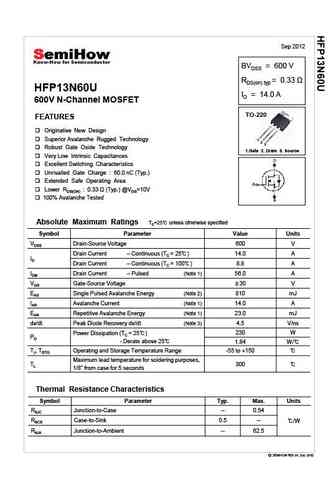
Sep 2012 BVDSS = 600 V RDS(on) typ = 0.33 HFP13N60U ID = 14.0 A 600V N-Channel MOSFET TO-220 FEATURES Originative New Design Superior Avalanche Rugged Technology 1 2 3 Robust Gate Oxide Technology 1.Gate 2. Drain 3. Source Very Low Intrinsic Capacitances Excellent Switching Characteristics Unrivalled Gate Charge 60.0 nC (Typ.) Extended Safe Operating Area
9.38. Size:629K convert
cs13n60p cs13n60f.pdf
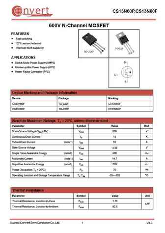
CS13N60P,CS13N60F nvert Suzhou Convert Semiconductor Co ., Ltd. 600V N-Channel MOSFET FEATURES Fast switching 100% avalanche tested Improved dv/dt capability APPLICATIONS Switch Mode Power Supply (SMPS) Uninterruptible Power Supply (UPS) Power Factor Correction (PFC) Device Marking and Package Information Device Package Marking CS13N60F TO-220F CS13N60F CS
9.39. Size:257K inchange semiconductor
fcp13n60n.pdf
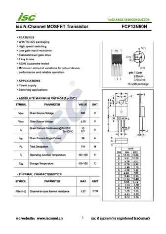
isc N-Channel MOSFET Transistor FCP13N60N FEATURES With TO-220 packaging High speed switching Low gate input resistance Standard level gate drive Easy to use 100% avalanche tested Minimum Lot-to-Lot variations for robust device performance and reliable operation APPLICATIONS Power supply Switching applications ABSOLUTE MAXIMUM RATINGS(T =25 ) a SYMBOL PA
9.40. Size:248K inchange semiconductor
fcpf13n60nt.pdf
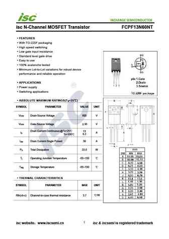
isc N-Channel MOSFET Transistor FCPF13N60NT FEATURES With TO-220F packaging High speed switching Low gate input resistance Standard level gate drive Easy to use 100% avalanche tested Minimum Lot-to-Lot variations for robust device performance and reliable operation APPLICATIONS Power supply Switching applications ABSOLUTE MAXIMUM RATINGS(T =25 ) a SYMBOL
Otros transistores... 11N10
, 11N10G
, 11P50A
, 12N50A
, 12N60A
, 12N60AF
, 13N110A
, 13N60A
, P60NF06
, 16N60A
, 16N60AF
, 16N60B
, 19MT050XFAPBF
, 1HN04CH
, 1HP04CH
, 1N60AF
, 1N60E
.
History: RCX081N20
| SGSP330
