30N20A Datasheet. Equivalente. Reemplazo. Hoja de especificaciones. Principales características
Número de Parte: 30N20A 📄📄
Tipo de FET: MOSFET
Polaridad de transistor: N
ESPECIFICACIONES MÁXIMAS
Pdⓘ - Máxima disipación de potencia: 300 W
|Vds|ⓘ - Voltaje máximo drenador-fuente: 200 V
|Vgs|ⓘ - Voltaje máximo fuente-puerta: 20 V
|Id|ⓘ - Corriente continua de drenaje: 30 A
Tjⓘ - Temperatura máxima de unión: 150 °C
CARACTERÍSTICAS ELÉCTRICAS
trⓘ - Tiempo de subida: 190 nS
Cossⓘ - Capacitancia de salida: 700 pF
RDSonⓘ - Resistencia estado encendido drenaje a fuente: 0.085 Ohm
Encapsulados: LCC
📄📄 Copiar
Búsqueda de reemplazo de 30N20A MOSFET
- Selecciónⓘ de transistores por parámetros
30N20A datasheet
..1. Size:34K microsemi
30n20a.pdf 
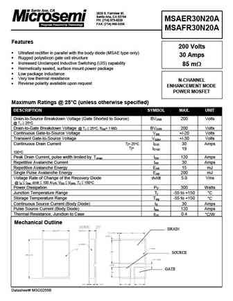
2830 S. Fairview St. Santa Ana, CA 92704 PH (714) 979-8220 MSAER30N20A FAX (714) 966-5256 MSAFR30N20A Features 200 Volts Ultrafast rectifier in parallel with the body diode (MSAE type only) 30 Amps Rugged polysilicon gate cell structure Increased Unclamped Inductive Switching (UIS) capability 85 m Hermetically sealed, surface mount power package Low pa
0.1. Size:42K microsemi
msaer30n20a msafr30n20a.pdf
2830 S. Fairview St. Santa Ana, CA 92704 PH (714) 979-8220 MSAER30N20A FAX (714) 966-5256 MSAFR30N20A Features 200 Volts Ultrafast rectifier in parallel with the body diode (MSAE type only) 30 Amps Rugged polysilicon gate cell structure Increased Unclamped Inductive Switching (UIS) capability 85 m Hermetically sealed, surface mount power package Low pa
9.1. Size:372K 1
cs30n20fa9r.pdf

Silicon N-Channel Power MOSFET R CS30N20F A9R General Description VDSS 200 V CS30N20F A9R, the silicon N-channel Enhanced ID 30 A PD(TC=25 ) 42 W VDMOSFETs, is obtained by the self-aligned planar Technology RDS(ON)Typ 70 m which reduce the conduction loss, improve switching performance and enhance the avalanche energy. The transistor can be used in various po
9.2. Size:138K international rectifier
irfs30n20d.pdf
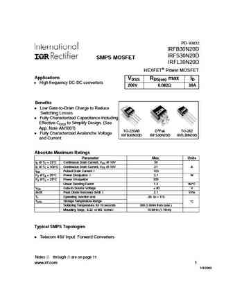
PD- 93832 IRFB30N20D IRFS30N20D SMPS MOSFET IRFL30N20D HEXFET Power MOSFET Applications VDSS RDS(on) max ID High frequency DC-DC converters 200V 0.082 30A Benefits Low Gate-to-Drain Charge to Reduce Switching Losses Fully Characterized Capacitance Including Effective COSS to Simplify Design, (See App. Note AN1001) TO-220AB D2Pak TO-262 Fully Characterized Avalanche Vo
9.3. Size:311K st
stw30n20.pdf
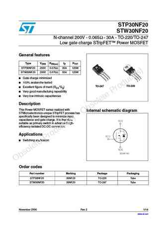
STP30NF20 STW30NF20 N-channel 200V - 0.065 - 30A - TO-220/TO-247 Low gate charge STripFET Power MOSFET General features Type VDSS RDS(on) ID PTOT STP30NF20 200V 0.075 30A 125W STW30NF20 200V 0.075 30A 125W Gate charge minimized 3 3 2 2 1 1 100% avalanche tested TO-220 TO-247 Excellent figure of merit (RDS*Qg) Very good manufactuing repeability Ver
9.4. Size:285K rohm
rnd030n20.pdf
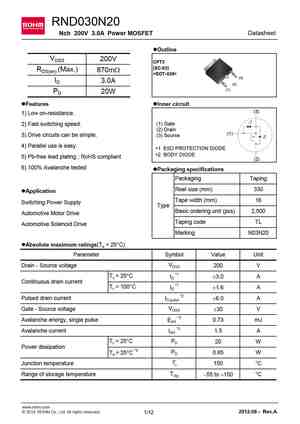
RND030N20 Nch 200V 3.0A Power MOSFET Datasheet Outline VDSS 200V CPT3 (SC-63) RDS(on) (Max.) 870m (3) ID 3.0A (2) (1) PD 20W Features Inner circuit (3) 1) Low on-resistance. 1 * (1) Gate 2) Fast switching speed. (2) Drain (1) 3) Drive circuits can be simple. (3) Source 2 * 4) Parallel use is easy. 1 ESD PROTECTION DIODE 2 BODY DIODE
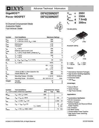
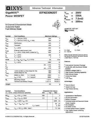
9.6. Size:126K ixys
ixth130n20t.pdf
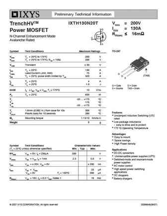
Preliminary Technical Information IXTH130N20T VDSS = 200V TrenchHVTM ID25 = 130A Power MOSFET RDS(on) 16m N-Channel Enhancement Mode Avalanche Rated Symbol Test Conditions Maximum Ratings TO-247 VDSS TJ = 25 C to 175 C 200 V VDGR TJ = 25 C to 175 C; RGS = 1M 200 V VGSM Transient 30 V ID25 TC = 25 C 130 A ILRMS Lead Current Limit, RMS
9.7. Size:170K ixys
ixtq130n20t.pdf
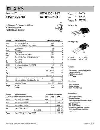
TrenchTM VDSS = 200V IXTQ130N20T ID25 = 130A Power MOSFET IXTH130N20T RDS(on) 16m N-Channel Enhancement Mode TO-3P (IXTQ) Avalanche Rated Fast Intrinsic Rectifier G D S Tab Symbol Test Conditions Maximum Ratings TO-247 ( IXTH) VDSS TJ = 25 C to 175 C 200 V VDGR TJ = 25 C to 175 C, RGS = 1M 200 V VGSS Continuous 20 V VGS
9.8. Size:180K ixys
mmix1f230n20t.pdf

Advance Technical Information GigaMOSTM TrenchTM VDSS = 200V MMIX1F230N20T HiperFETTM ID25 = 168A Power MOSFET RDS(on) 8.3m trr 200ns (Electrically Isolated Tab) D N-Channel Enhancement Mode G Avalanche Rated Fast Intrinsic Diode S Symbol Test Conditions Maximum Ratings Isolated Tab VDSS TJ = 25 C to 175 C 200 V
9.10. Size:78K onsemi
ntb30n20.pdf
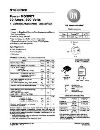
NTB30N20 Power MOSFET 30 Amps, 200 Volts N-Channel Enhancement-Mode D2PAK http //onsemi.com Features Source-to-Drain Diode Recovery Time Comparable to a Discrete VDSS RDS(ON) TYP ID MAX Fast Recovery Diode Avalanche Energy Specified 200 V 68 mW @ VGS = 10 V 30 A IDSS and RDS(on) Specified at Elevated Temperature Mounting Information Provided for the D2PAK Package N-
9.11. Size:158K onsemi
ntp30n20 ntp30n20g.pdf
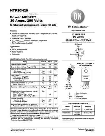
NTP30N20 Preferred Device Power MOSFET 30 Amps, 200 Volts N-Channel Enhancement-Mode TO-220 http //onsemi.com Features Source-to-Drain Diode Recovery Time Comparable to a Discrete 30 AMPERES Fast Recovery Diode 200 VOLTS Avalanche Energy Specified 68 mW @ VGS = 10 V (Typ) IDSS and RDS(on) Specified at Elevated Temperature Pb-Free Package is Available* N-Channel D
9.12. Size:138K secos
ssrf30n20-400.pdf
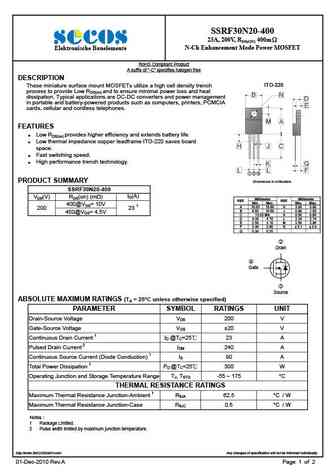
SSRF30N20-400 23A, 200V, RDS(ON) 400m N-Ch Enhancement Mode Power MOSFET Elektronische Bauelemente RoHS Compliant Product A suffix of -C specifies halogen free DESCRIPTION These miniature surface mount MOSFETs utilize a high cell density trench ITO-220 process to provide Low RDS(on) and to ensure minimal power loss and heat B N dissipation. Typical applications are DC-
9.13. Size:307K analog power
am30n20-400pcfm.pdf
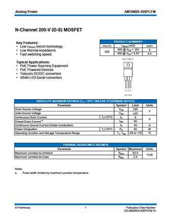
Analog Power AM30N20-400PCFM N-Channel 200-V (D-S) MOSFET PRODUCT SUMMARY Key Features rDS(on) (m ) VDS (V) ID(A) Low r trench technology DS(on) 400 @ VGS = 10V 9 Low thermal impedance 200 450 @ VGS = 5.5V 8.5 Fast switching speed Typical Applications PoE Power Sourcing Equipment PoE Powered Devices Telecom DC/DC converters White LED bo
9.14. Size:85K analog power
am30n20-78d.pdf

Analog Power AM30N20-78D N-Channel 200-V (D-S) MOSFET These miniature surface mount MOSFETs utilize a PRODUCT SUMMARY high cell density trench process to provide low VDS (V) rDS(on) m( ) ID (A) rDS(on) and to ensure minimal power loss and heat dissipation. Typical applications are DC-DC 78 @ VGS = 10V 21 converters and power management in portable and 200 92 @ VGS = 5.5V 20 bat
9.15. Size:341K cystek
mte130n20fp.pdf
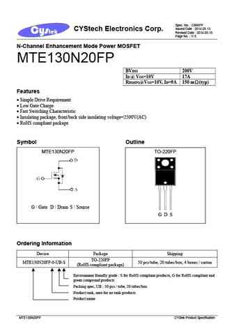
Spec. No. C966FP Issued Date 2014.05.13 CYStech Electronics Corp. Revised Date 2014.05.15 Page No. 1/ 8 N-Channel Enhancement Mode Power MOSFET MTE130N20FP BVDSS 200V ID @ VGS=10V 17A RDS(ON)@VGS=10V, ID=9A 150 m (typ) Features Simple Drive Requirement Low Gate Charge Fast Switching Characteristic Insulating package, front/back side insulating v
9.16. Size:394K cystek
mte130n20kj3.pdf
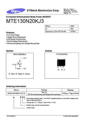
Spec. No. C952J3 Issued Date 2014.02.27 CYStech Electronics Corp. Revised Date 2014.03.05 Page No. 1/9 N-Channel Enhancement Mode Power MOSFET MTE130N20KJ3 BVDSS 200V ID 18A 142m RDSON(TYP) @ VGS=10V, ID=9A Features Low Gate Charge Simple Drive Requirement ESD Diode Protected Gate Fast Switching Characteristic Pb-free lead plating and
9.17. Size:296K cystek
mte130n20kfp.pdf
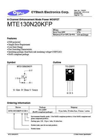
Spec. No. C952FP Issued Date 2013.12.24 CYStech Electronics Corp. Revised Date Page No. 1/ 8 N-Channel Enhancement Mode Power MOSFET MTE130N20KFP BVDSS 200V ID @ VGS=10V 17A RDS(ON)@VGS=10V, ID=9A 134 m (typ) Features ESD protected Simple Drive Requirement Low Gate Charge Fast Switching Characteristic Insulating package, front/back side in
9.18. Size:369K cystek
mte130n20j3.pdf
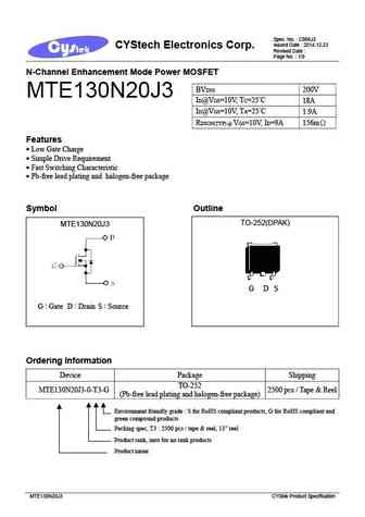
Spec. No. C966J3 Issued Date 2014.12.23 CYStech Electronics Corp. Revised Date Page No. 1/9 N-Channel Enhancement Mode Power MOSFET BVDSS 200V MTE130N20J3 ID@VGS=10V, TC=25 C 18A ID@VGS=10V, TA=25 C 1.9A 156m RDSON(TYP) @ VGS=10V, ID=9A Features Low Gate Charge Simple Drive Requirement Fast Switching Characteristic Pb-free lead pla
9.19. Size:337K cystek
mte130n20kf3.pdf
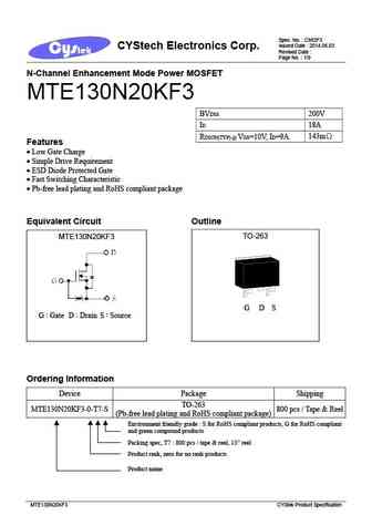
Spec. No. C952F3 Issued Date 2014.06.03 CYStech Electronics Corp. Revised Date Page No. 1/9 N-Channel Enhancement Mode Power MOSFET MTE130N20KF3 BVDSS 200V ID 18A 143m RDSON(TYP) @ VGS=10V, ID=9A Features Low Gate Charge Simple Drive Requirement ESD Diode Protected Gate Fast Switching Characteristic Pb-free lead plating and RoHS compli
9.20. Size:355K cystek
mte130n20ke3.pdf
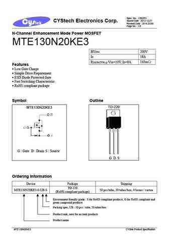
Spec. No. C952E3 Issued Date 2013.12.27 CYStech Electronics Corp. Revised Date 2014.03.05 Page No. 1/8 N-Channel Enhancement Mode Power MOSFET MTE130N20KE3 BVDSS 200V ID 18A 143m RDSON(TYP) @ VGS=10V, ID=9A Features Low Gate Charge Simple Drive Requirement ESD Diode Protected Gate Fast Switching Characteristic RoHS compliant package
9.21. Size:4018K goford
g30n20k g30n20t g30n20f.pdf

GOFORD G30N20 Description The G30N20 uses advanced trench technology and design to provide excellent RDS(ON) with low gate charge. It can be used in a wide variety of applications. General Features VDSS RDS(ON) ID @ 10V (Typ) 200V 62m 30A Schematic diagram High density cell design for ultra low Rdson Fully characterized avalanche voltage and current
9.22. Size:22K shaanxi
wvm30n20.pdf

Shaanxi Qunli Electric Co., Ltd Add. No. 1 Qunli Road,Baoji City,Shaanxi,China WVM30N20 Power MOSFET(N-channel) Transistor Features 1. It s voltage control component with good input impedance, small starting power dissipation, wide area of safe operation, good temperature stability. 2. Implementation of standards GJB33A-97, QZJ840611 3. Use for high speed switch, circuit of powe
9.23. Size:1479K cn vbsemi
30n20.pdf
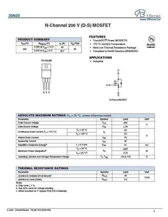
30N20 www.VBsemi.tw N-Channel 200 V (D-S) MOSFET FEATURES PRODUCT SUMMARY TrenchFET Power MOSFETS VDS (V) RDS(on) ( ) ID (A) Qg (Typ) 175 C Junction Temperature RoHS 0.060 at VGS = 10 V COMPLIANT 40 New Low Thermal Resistance Package 200 95 0.070 at VGS = 6 V 38.7 Compliant to RoHS Directive 2002/95/EC APPLICATIONS TO-220AB Industrial D G G D S
9.24. Size:5229K cn apm
ap130n20mp.pdf
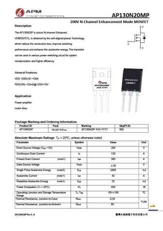
AP130N20MP 200V N-Channel Enhancement Mode MOSFET Description The AP130N20P is silicon N-channel Enhanced VDMOSFETs, is obtained by the self-aligned planar Technology which reduce the conduction loss, improve switching performance and enhance the avalanche energy. The transistor can be used in various power switching circuit for system miniaturization and higher efficiency. G
9.25. Size:1255K cn apm
ap30n20p.pdf
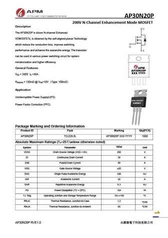
AP30N20P 200V N-Channel Enhancement Mode MOSFET Description The AP30N20P is silicon N-channel Enhanced VDMOSFETs, is obtained by the self-aligned planar Technology which reduce the conduction loss, improve switching performance and enhance the avalanche energy. The transistor can be used in various power switching circuit for system miniaturization and higher efficiency. Gener
Otros transistores... 1N60F, 1N60G, 20N50B, 20N60A, 24N50A, 24N50B, 24N50C, 2MI50S-050, MMIS60R580P, 38N10A, BCS4N10, BFC60, BFD63, BFD71, BFD77, BFD82, BFD88