75N10 Datasheet. Equivalente. Reemplazo. Hoja de especificaciones. Principales características
Número de Parte: 75N10 📄📄
Tipo de FET: MOSFET
Polaridad de transistor: N
ESPECIFICACIONES MÁXIMAS
Pdⓘ - Máxima disipación de potencia: 300 W
|Vds|ⓘ - Voltaje máximo drenador-fuente: 100 V
|Vgs|ⓘ - Voltaje máximo fuente-puerta: 20 V
|Id|ⓘ - Corriente continua de drenaje: 75 A
Tjⓘ - Temperatura máxima de unión: 150 °C
CARACTERÍSTICAS ELÉCTRICAS
trⓘ - Tiempo de subida: 110 nS
RDSonⓘ - Resistencia estado encendido drenaje a fuente: 0.02 Ohm
Encapsulados: TO-3
📄📄 Copiar
Búsqueda de reemplazo de 75N10 MOSFET
- Selecciónⓘ de transistores por parámetros
75N10 datasheet
..1. Size:228K inchange semiconductor
75n10.pdf 
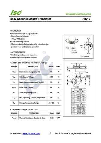
INCHANGE Semiconductor isc N-Channel Mosfet Transistor 75N10 FEATURES Drain Current I = 75A@ T =25 D C Drain Source Voltage- V =100V(Min) DSS Fast Switching Speed Minimum Lot-to-Lot variations for robust device performance and reliable operation APPLICATIONS Switching mode power supplies General purpose power amplifier ABSOLUTE MAXIMUM RATINGS(T =25 ) a
0.1. Size:1354K rohm
rsd175n10fra.pdf
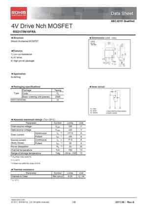
Data Sheet AEC-Q101 Qualified 4V Drive Nch MOSFET RSD175N10 RSD175N10FRA Structure Dimensions (Unit mm) Silicon N-channel MOSFET CPT3 6.5 (SC-63) 5.1 2.3 0.5 Features 1) Low on-resistance. 4) 4V drive. 0.75 4) High power package. 0.65 0.9 2.3 (1) (2) (3) 2.3 0.5 1.0 Application Switching Packaging specifications Inner circuit 1
0.2. Size:1159K rohm
rsd175n10.pdf
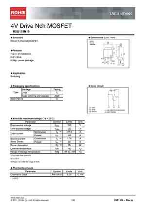
Data Sheet 4V Drive Nch MOSFET RSD175N10 Structure Dimensions (Unit mm) Silicon N-channel MOSFET CPT3 6.5 (SC-63) 5.1 2.3 0.5 Features 1) Low on-resistance. 4) 4V drive. 0.75 4) High power package. 0.65 0.9 2.3 (1) (2) (3) 2.3 0.5 1.0 Application Switching Packaging specifications Inner circuit 1 Package Taping Type Code TL Bas
0.3. Size:151K ixys
ixfh75n10q ixft75n10q.pdf
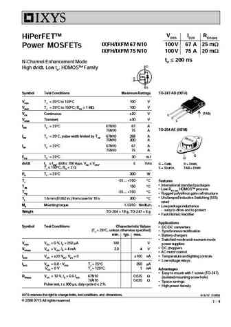
Advanced Technical Information IXFH 75N10Q VDSS = 100 V HiPerFETTM IXFT 75N10Q ID25 = 75 A Power MOSFETs RDS(on) = 20 mW Q-Class t 200ns rr N-Channel Enhancement Mode Avalanche Rated, High dv/dt Low Gate Charge and Capacitances Symbol Test Conditions Maximum Ratings TO-247 AD (IXFH) VDSS TJ = 25 C to 150 C 100 V VDGR TJ = 25 C to 150 C; RGS = 1 M 100 V VGS Continuous
0.4. Size:252K ixys
ixta75n10p ixtp75n10p ixtq75n10p.pdf
IXTA 75N10P VDSS = 100 V PolarHTTM IXTP 75N10P ID25 = 75 A Power MOSFET IXTQ 75N10P RDS(on) 25 m N-Channel Enhancement Mode Avalanche Rated TO-263 (IXTA) Symbol Test Conditions Maximum Ratings G S VDSS TJ = 25 C to 175 C 100 V (TAB) VDGR TJ = 25 C to 175 C; RGS = 1 M 100 V VGS Continuous 20 V TO-220 (IXTP) VGSM Transient
0.5. Size:579K ixys
ixth67n10 ixtm67n10 ixth75n10 ixtm75n10 ixtt75n10.pdf
VDSS ID25 RDS(on) MegaMOSTMFET IXTH / IXTM 67N10 100 V 67 A 25 m IXTH / IXTM 75N10 100 V 75 A 20 m IXTT 75N10 N-Channel Enhancement Mode TO-247 AD (IXTH) Symbol Test Conditions Maximum Ratings (TAB) VDSS TJ = 25 C to 150 C 100 V VDGR TJ = 25 C to 150 C; RGS = 1 M 100 V TO-204 AE (IXTM) VGS Continuous 20 V VGSM Transient 30
0.6. Size:139K ixys
ixth75n10l2 ixtt75n10l2.pdf
Advance Technical Information LinearL2TM Power VDSS = 100V IXTH75N10L2 MOSFET w/extended ID25 = 75A IXTT75N10L2 RDS(on) 21m FBSOA D D D D O D O N-Channel Enhancement Mode RGi Guaranteed FBSOA w w G O Avalanche Rated TO-247 (IXTH) O S Symbol Test Conditions Maximum Ratings G VDSS TJ = 25 C to 150 C 100 V D D (Tab) S VDGR TJ = 25
0.8. Size:34K microsemi
msafx75n10a.pdf
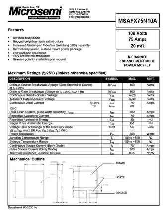
2830 S. Fairview St. Santa Ana, CA 92704 PH (714) 979-8220 FAX (714) 966-5256 MSAFX75N10A Features 100 Volts Ultrafast body diode 75 Amps Rugged polysilicon gate cell structure Increased Unclamped Inductive Switching (UIS) capability 20 m Hermetically sealed, surface mount power package Low package inductance Very low thermal resistance N-CHANNEL
0.9. Size:82K microsemi
msafa75n10c.pdf
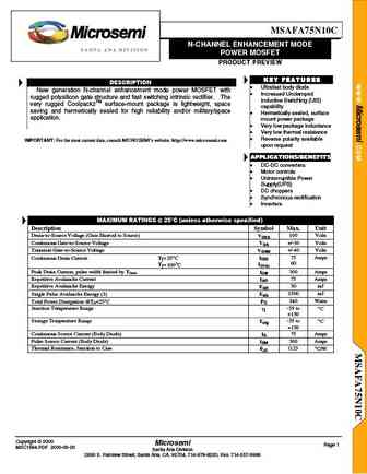
MSAFA75N10C N-CHANNEL ENHANCEMENT MODE SANTA ANA DIVISION POWER MOSFET PRODUCT PREVIEW KEY FEATURES KEY FEATURES KEY FEATURES KEY FEATURES DESCRIPTION Ultrafast body diode New generation N-channel enhancement mode power MOSFET with Increased Unclamped rugged polysilicon gate structure and fast switching intrinsic rectifier. The Inductive Switching (UIS) very
0.10. Size:857K cet
cep75n10 ceb75n10.pdf
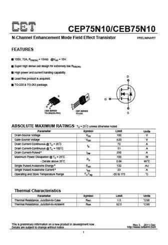
CEP75N10/CEB75N10 N-Channel Enhancement Mode Field Effect Transistor PRELIMINARY FEATURES 100V, 72A, RDS(ON) = 15m @VGS = 10V. Super high dense cell design for extremely low RDS(ON). High power and current handing capability. D Lead free product is acquired. TO-220 & TO-263 package. G CEB SERIES CEP SERIES TO-263(DD-PAK) S TO-220 ABSOLUTE MAXIMUM RATINGS Tc = 25 C unless otherw
0.14. Size:385K nell
75n10a 75n10b.pdf
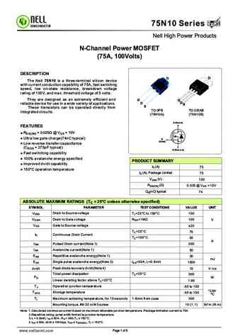
RoHS 75N10 Series RoHS SEMICONDUCTOR Nell High Power Products N-Channel Power MOSFET (75A, 100Volts) DESCRIPTION D D The Nell 75N10 is a three-terminal silicon device with current conduction capability of 75A, fast switching speed, low on-state resistance, breakdown voltage rating of 100V, and max. threshold voltage of 5 volts. They are designed as an extremely efficient and G
0.15. Size:1003K belling
blp075n10g-p blp075n10g-b.pdf
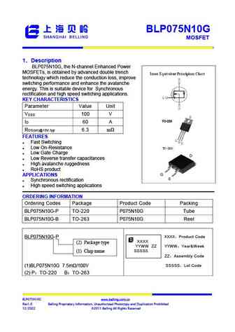
BLP075N10G MOSFET Step-Down Converter , 1 Description BLP075N10G, the N-channel Enhanced Power MOSFETs, is obtained by advanced double trench technology which reduce the conduction loss, improve switching performance and enhance the avalanche energy. This is suitable device for Synchronous rectification and high speed switching applications. KEY CHARACTERISTICS Param
0.17. Size:216K hy
hy75n10t.pdf
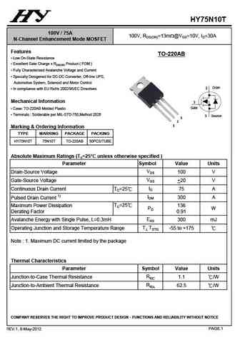
HY75N10T 100V / 75A 100V, RDS(ON)=13mW@VGS=10V, ID=30A N-Channel Enhancement Mode MOSFET Features TO-220AB Low On-State Resistance Excellent Gate Charge x RDS(ON) Product ( FOM ) Fully Characterized Avalanche Voltage and Current Specially Desigened for DC-DC Converter, Off-line UPS, Automotive System, Solenoid and Motor Control Drain 2 In compliance with E
0.18. Size:784K way-on
wms175n10hg4.pdf
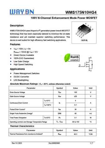
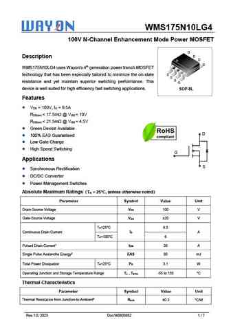
WMS175N10HG4 100V N-Channel Enhancement Mode Power MOSFET D D Description D D WMS175N10HG4 uses Wayon's 4th generation power trench MOSFET technology that has been especially tailored to minimize the on-state S S S resistance and yet maintain superior switching performance. This G device is well suited for high efficiency fast switching applications. SOP-8L Features
0.19. Size:614K way-on
wmo175n10lg4.pdf
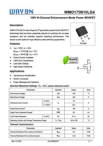
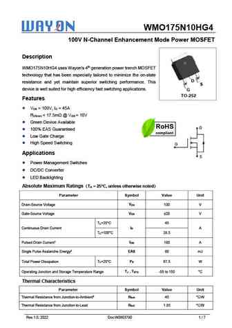
WMO175N10LG4 100V N-Channel Enhancement Mode Power MOSFET Description WMO175N10LG4 uses Wayon's 4th generation power trench MOSFET technology that has been especially tailored to minimize the on-state resistance and yet maintain superior switching performance. This D S device is well suited for high efficiency fast switching applications. G TO-252 Features V = 100V, I =
0.20. Size:620K way-on
wmb175n10lg4.pdf
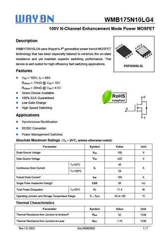
WMB175N10LG4 100V N-Channel Enhancement Mode Power MOSFET Description D D D DD D D D WMB175N10LG4 uses Wayon's 4th generation power trench MOSFET G technology that has been especially tailored to minimize the on-state ss s ss G s resistance and yet maintain superior switching performance. This device is well suited for high efficiency fast switching applications. PDFN50
0.21. Size:599K way-on
wmk175n10hg4.pdf
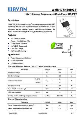
WMK175N10HG4 100V N-Channel Enhancement Mode Power MOSFET Description WMK175N10HG4 uses Wayon's 4th generation power trench MOSFET technology that has been especially tailored to minimize the on-state resistance and yet maintain superior switching performance. This device is well suited for high efficiency fast switching applications. S D G Features TO-220 V = 100V, I =
0.22. Size:604K way-on
wmk175n10lg4.pdf
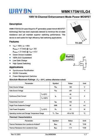
WMK175N10LG4 100V N-Channel Enhancement Mode Power MOSFET Description WMK175N10LG4 uses Wayon's 4th generation power trench MOSFET technology that has been especially tailored to minimize the on-state resistance and yet maintain superior switching performance. This device is well suited for high efficiency fast switching applications. S D G Features TO-220 V = 100V, I =
0.23. Size:617K way-on
wmb175n10hg4.pdf
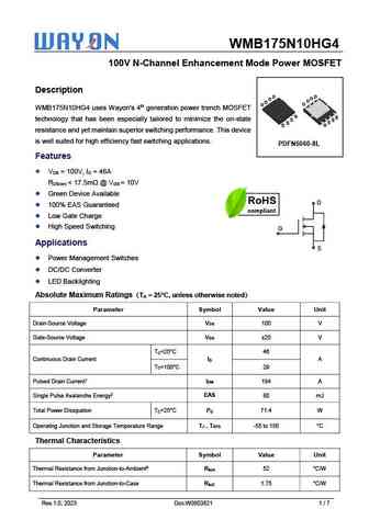
WMB175N10HG4 100V N-Channel Enhancement Mode Power MOSFET Description D D D DD D D D WMB175N10HG4 uses Wayon's 4th generation power trench MOSFET G technology that has been especially tailored to minimize the on-state ss s ss G s resistance and yet maintain superior switching performance. This device is well suited for high efficiency fast switching applications. PDFN50
0.24. Size:600K way-on
wmq175n10lg4.pdf
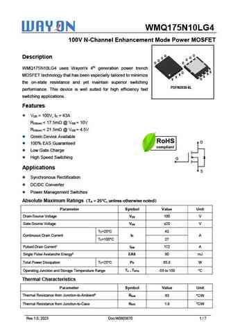
WMQ175N10LG4 100V N-Channel Enhancement Mode Power MOSFET D D Description D D D D D D WMQ175N10LG4 uses Wayon's 4th generation power trench S G S S MOSFET technology that has been especially tailored to minimize S S G S the on-state resistance and yet maintain superior switching PDFN3030-8L performance. This device is well suited for high efficiency fast switching
0.25. Size:622K way-on
wmq175n10hg4.pdf
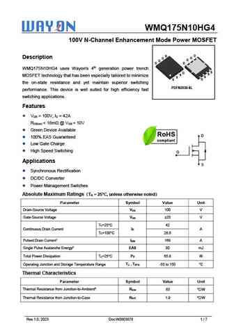
WMQ175N10HG4 100V N-Channel Enhancement Mode Power MOSFET D D Description D D D D D D WMQ175N10HG4 uses Wayon's 4th generation power trench S G S S MOSFET technology that has been especially tailored to minimize S S G S the on-state resistance and yet maintain superior switching PDFN3030-8L performance. This device is well suited for high efficiency fast switching
0.26. Size:609K way-on
wmo175n10hg4.pdf
WMO175N10HG4 100V N-Channel Enhancement Mode Power MOSFET Description WMO175N10HG4 uses Wayon's 4th generation power trench MOSFET technology that has been especially tailored to minimize the on-state D resistance and yet maintain superior switching performance. This S device is well suited for high efficiency fast switching applications. G TO-252 Features V = 100V, I =
0.27. Size:770K way-on
wms175n10lg4.pdf
WMS175N10LG4 100V N-Channel Enhancement Mode Power MOSFET D D Description D D WMS175N10LG4 uses Wayon's 4th generation power trench MOSFET technology that has been especially tailored to minimize the on-state S S S resistance and yet maintain superior switching performance. This G device is well suited for high efficiency fast switching applications. SOP-8L Features
0.28. Size:216K inchange semiconductor
ixta75n10p.pdf
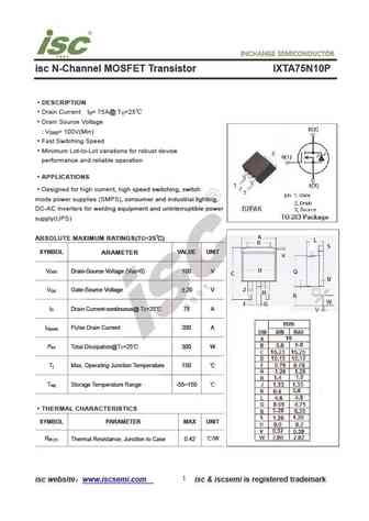
isc N-Channel MOSFET Transistor IXTA75N10P DESCRIPTION Drain Current I = 75A@ T =25 D C Drain Source Voltage V = 100V(Min) DSS Fast Switching Speed Minimum Lot-to-Lot variations for robust device performance and reliable operation APPLICATIONS . Designed for high current, high speed switching, switch mode power supplies (SMPS), consumer and industrial lighting, D
Otros transistores... 40N10, 50N15, 60N05, 60N05-16, 60N06-18, 60N10, 6N70A, 75N06, SKD502T, 75NF75, BUK436-100A, BUK436-100B, BUK436-200A, BUK436-200B, BUK436-60A, BUK436-60B, BUK436-800A