IPP12CN10N MOSFET Equivalente. Reemplazo. Hoja de especificaciones. Principales características
Número de Parte: IPP12CN10N
Tipo de FET: MOSFET
Polaridad de transistor: N
ESPECIFICACIONES MÁXIMAS
Pdⓘ - Máxima disipación de potencia: 125 W
|Vds|ⓘ - Voltaje máximo drenador-fuente: 100 V
|Vgs|ⓘ - Voltaje máximo fuente-puerta: 20 V
|Id|ⓘ - Corriente continua de drenaje: 67 A
Tjⓘ - Temperatura máxima de unión: 175 °C
CARACTERÍSTICAS ELÉCTRICAS
trⓘ - Tiempo de subida: 21 nS
Cossⓘ - Capacitancia de salida: 489 pF
RDSonⓘ - Resistencia estado encendido drenaje a fuente: 0.0129 Ohm
Encapsulados: TO220
Búsqueda de reemplazo de IPP12CN10N MOSFET
- Selecciónⓘ de transistores por parámetros
IPP12CN10N datasheet
ipp12cn10n.pdf
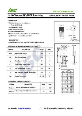
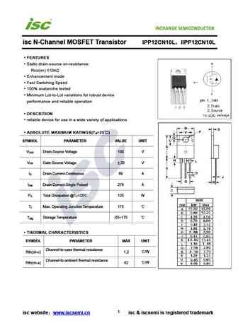
INCHANGE Semiconductor isc N-Channel MOSFET Transistor IPP12CN10N IIPP12CN10N FEATURES Static drain-source on-resistance RDS(on) 12.9m Enhancement mode Fast Switching Speed 100% avalanche tested Minimum Lot-to-Lot variations for robust device performance and reliable operation DESCRITION reliable device for use in a wide variety of applications ABSOLUTE MA
ipb12cn10ng ipd12cn10ng ipi12cn10ng ipp12cn10ng ipb12cn10ng ipi12cn10ng.pdf
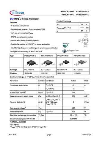
IPB12CN10N G IPD12CN10N G IPI12CN10N G IPP12CN10N G OptiMOS 2 Power-Transistor Product Summary Features VDS 100 V N-channel, normal level RDS(on),max (TO252) 12.4 mW Excellent gate charge x R product (FOM) DS(on) ID 67 A Very low on-resistance R DS(on) 175 C operating temperature Pb-free lead plating; RoHS compliant Qualified according to JEDEC1)
ipb12cn10n-g ipd12cn10n-g ipi12cn10n-g ipp12cn10n-g.pdf
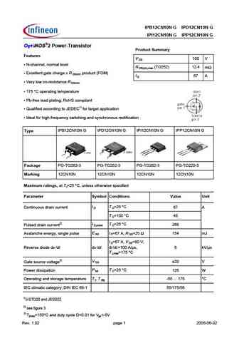
IPB12CN10N G IPD12CN10N G IPI12CN10N G IPP12CN10N G OptiMOS 2 Power-Transistor Product Summary Features V 100 V DS N-channel, normal level R (TO252) 12.4 m DS(on),max Excellent gate charge x R product (FOM) DS(on) I 67 A D Very low on-resistance R DS(on) 175 C operating temperature Pb-free lead plating; RoHS compliant Qualified according to JEDEC
ipp12cn10l-g ips12cn10l-g.pdf
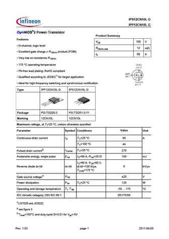
IPS12CN10L G IPP12CN10L G OptiMOS 2 Power-Transistor Product Summary Features VDS 100 V N-channel, logic level RDS(on),max 12 mW Excellent gate charge x R product (FOM) DS(on) ID 69 A Very low on-resistance R DS(on) 175 C operating temperature Pb-free lead plating; RoHS compliant Qualified according to JEDEC1) for target application Ideal for high
Otros transistores... IPP048N04N , IPP052NE7N3 , IPP062NE7N3 , IPP065N03L , IPP072N10N3 , IPP084N06L3 , IPP086N10N3 , IPP126N10N3 , 7N60 , IPP180N10N3 , IPP26CN10N , IPP35CN10N , IPP80CN10N , IPW60R060C7 , IPW60R070CFD7 , IPW60R080P7 , IPW60R099P7 .
History: WMM80R1K0S
History: WMM80R1K0S
🌐 : EN ES РУ

Liste
Recientemente añadidas las descripciónes de los transistores:
MOSFET: AUB034N10 | AUB033N08BG | AUB026N085 | AUA062N08BG | AUA060N08AG | AUA056N08BGL | AUA039N10 | ASW80R290E | ASW65R120EFD | ASW65R110E | ASW65R095EFD | ASW65R046EFD | ASW65R041EFDA | ASW65R041E | ASW60R150E | ASW60R090EFDA
Popular searches
a92 transistor | rfp50n06 | bd140 datasheet | tip2955 | tip35 | 2sk117 | irf9540n datasheet | ss8050