IPP12CN10N Specs and Replacement
Type Designator: IPP12CN10N
Type of Transistor: MOSFET
Type of Control Channel: N-Channel
Absolute Maximum Ratings
Pd ⓘ - Maximum Power Dissipation: 125 W
|Vds|ⓘ - Maximum Drain-Source Voltage: 100 V
|Vgs|ⓘ - Maximum Gate-Source Voltage: 20 V
|Id| ⓘ - Maximum Drain Current: 67 A
Tj ⓘ - Maximum Junction Temperature: 175 °C
Electrical Characteristics
tr ⓘ - Rise Time: 21 nS
Cossⓘ - Output Capacitance: 489 pF
RDSonⓘ - Maximum Drain-Source On-State Resistance: 0.0129 Ohm
Package: TO220
IPP12CN10N substitution
- MOSFET ⓘ Cross-Reference Search
IPP12CN10N datasheet
ipp12cn10n.pdf
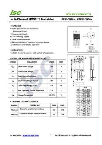
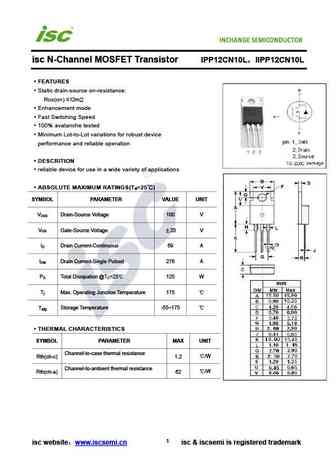
INCHANGE Semiconductor isc N-Channel MOSFET Transistor IPP12CN10N IIPP12CN10N FEATURES Static drain-source on-resistance RDS(on) 12.9m Enhancement mode Fast Switching Speed 100% avalanche tested Minimum Lot-to-Lot variations for robust device performance and reliable operation DESCRITION reliable device for use in a wide variety of applications ABSOLUTE MA... See More ⇒
ipb12cn10ng ipd12cn10ng ipi12cn10ng ipp12cn10ng ipb12cn10ng ipi12cn10ng.pdf
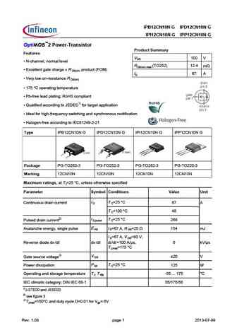
IPB12CN10N G IPD12CN10N G IPI12CN10N G IPP12CN10N G OptiMOS 2 Power-Transistor Product Summary Features VDS 100 V N-channel, normal level RDS(on),max (TO252) 12.4 mW Excellent gate charge x R product (FOM) DS(on) ID 67 A Very low on-resistance R DS(on) 175 C operating temperature Pb-free lead plating; RoHS compliant Qualified according to JEDEC1)... See More ⇒
ipb12cn10n-g ipd12cn10n-g ipi12cn10n-g ipp12cn10n-g.pdf
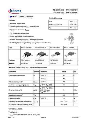
IPB12CN10N G IPD12CN10N G IPI12CN10N G IPP12CN10N G OptiMOS 2 Power-Transistor Product Summary Features V 100 V DS N-channel, normal level R (TO252) 12.4 m DS(on),max Excellent gate charge x R product (FOM) DS(on) I 67 A D Very low on-resistance R DS(on) 175 C operating temperature Pb-free lead plating; RoHS compliant Qualified according to JEDEC... See More ⇒
ipp12cn10l-g ips12cn10l-g.pdf
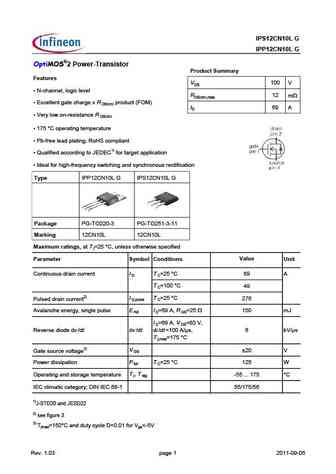
IPS12CN10L G IPP12CN10L G OptiMOS 2 Power-Transistor Product Summary Features VDS 100 V N-channel, logic level RDS(on),max 12 mW Excellent gate charge x R product (FOM) DS(on) ID 69 A Very low on-resistance R DS(on) 175 C operating temperature Pb-free lead plating; RoHS compliant Qualified according to JEDEC1) for target application Ideal for high... See More ⇒
Detailed specifications: IPP048N04N, IPP052NE7N3, IPP062NE7N3, IPP065N03L, IPP072N10N3, IPP084N06L3, IPP086N10N3, IPP126N10N3, 7N60, IPP180N10N3, IPP26CN10N, IPP35CN10N, IPP80CN10N, IPW60R060C7, IPW60R070CFD7, IPW60R080P7, IPW60R099P7
Keywords - IPP12CN10N MOSFET specs
IPP12CN10N cross reference
IPP12CN10N equivalent finder
IPP12CN10N pdf lookup
IPP12CN10N substitution
IPP12CN10N replacement
Can't find your MOSFET? Learn how to find a substitute transistor by analyzing voltage, current and package compatibility
History: LSD65R380GT | IRFH5302 | TK290A65Y | IRLP3034 | IRLML2060
🌐 : EN ES РУ

LIST
Last Update
MOSFET: AUB034N10 | AUB033N08BG | AUB026N085 | AUA062N08BG | AUA060N08AG | AUA056N08BGL | AUA039N10 | ASW80R290E | ASW65R120EFD | ASW65R110E
Popular searches
a92 transistor | rfp50n06 | bd140 datasheet | tip2955 | tip35 | 2sk117 | irf9540n datasheet | ss8050