SFW9610 MOSFET Equivalente. Reemplazo. Hoja de especificaciones. Principales características
Número de Parte: SFW9610
Tipo de FET: MOSFET
Polaridad de transistor: P
ESPECIFICACIONES MÁXIMAS
Pdⓘ - Máxima
disipación de potencia: 20 W
|Vds|ⓘ - Voltaje máximo drenador-fuente: 200 V
|Vgs|ⓘ - Voltaje máximo fuente-puerta: 30 V
|Id|ⓘ - Corriente continua
de drenaje: 1.75 A
Tjⓘ - Temperatura máxima de unión: 150 °C
CARACTERÍSTICAS ELÉCTRICAS
trⓘ - Tiempo
de subida: 20 nS
Cossⓘ - Capacitancia de salida: 45 pF
RDSonⓘ - Resistencia estado encendido drenaje a fuente: 3 Ohm
Encapsulados: TO263
Búsqueda de reemplazo de SFW9610 MOSFET
- Selecciónⓘ de transistores por parámetros
SFW9610 datasheet
..1. Size:254K fairchild semi
sfi9610 sfw9610.pdf 

SFW/I9610 Advanced Power MOSFET FEATURES BVDSS = -200 V Avalanche Rugged Technology RDS(on) = 3.0 Rugged Gate Oxide Technology Lower Input Capacitance ID = -1.75 A Improved Gate Charge Extended Safe Operating Area D2-PAK I2-PAK Lower Leakage Current 10 A (Max.) @ VDS = -200V 2 Low RDS(ON) 2.084 (Typ.) 1 1 2 3 3 1. Gate 2. Drain 3. Source Absolute Maxi
..2. Size:497K samsung
sfw9610.pdf

Advanced Power MOSFET FEATURES BVDSS = -200 V Avalanche Rugged Technology RDS(on) = 3.0 Rugged Gate Oxide Technology Lower Input Capacitance ID = -1.75 A Improved Gate Charge Extended Safe Operating Area Lower Leakage Current 10 A (Max.) @ VDS = -200V 2 Low RDS(ON) 2.084 (Typ.) 1 1 2 3 3 1. Gate 2. Drain 3. Source Absolute Maximum Ratings Symbol Ch
8.1. Size:506K samsung
sfw9614.pdf
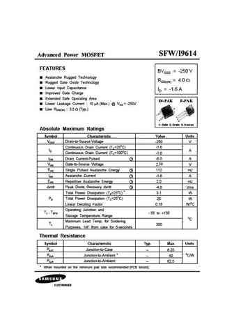
Advanced Power MOSFET FEATURES BVDSS = -250 V Avalanche Rugged Technology RDS(on) = 4.0 Rugged Gate Oxide Technology Lower Input Capacitance ID = -1.6 A Improved Gate Charge Extended Safe Operating Area Lower Leakage Current 10 A (Max.) @ VDS = -250V 2 Low RDS(ON) 3.5 (Typ.) 1 1 2 3 3 1. Gate 2. Drain 3. Source Absolute Maximum Ratings Symbol Char
9.1. Size:259K fairchild semi
sfi9624 sfw9624.pdf

SFW/I9624 Advanced Power MOSFET FEATURES BVDSS = -250 V Avalanche Rugged Technology RDS(on) = 2.4 Rugged Gate Oxide Technology Lower Input Capacitance ID = -2.7 A Improved Gate Charge Extended Safe Operating Area D2-PAK I2-PAK Lower Leakage Current 10 A (Max.) @ VDS = -250V 2 Low RDS(ON) 1.65 (Typ.) 1 1 2 3 3 1. Gate 2. Drain 3. Source Absolute Maximum
9.2. Size:259K fairchild semi
sfw9640tm.pdf

SFW/I9640 Advanced Power MOSFET FEATURES BVDSS = -200 V Avalanche Rugged Technology RDS(on) = 0.5 Rugged Gate Oxide Technology Lower Input Capacitance ID = -11 A Improved Gate Charge Extended Safe Operating Area D2-PAK I2-PAK Lower Leakage Current 10 A (Max.) @ VDS = -200V 2 Low RDS(ON) 0.344 (Typ.) 1 1 2 3 3 1. Gate 2. Drain 3. Source Absolute Maximum
9.3. Size:256K fairchild semi
sfi9630 sfw9630.pdf

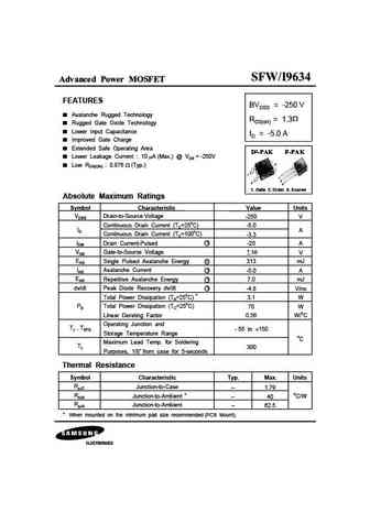
SFW/I9630 Advanced Power MOSFET FEATURES BVDSS = -200 V Avalanche Rugged Technology RDS(on) = 0.8 Rugged Gate Oxide Technology Lower Input Capacitance ID = -6.5 A Improved Gate Charge Extended Safe Operating Area D2-PAK I2-PAK Lower Leakage Current 10 A (Max.) @ VDS = -200V 2 Low RDS(ON) 0.581 (Typ.) 1 1 2 3 3 1. Gate 2. Drain 3. Source Absolute Maximu
9.4. Size:263K fairchild semi
sfi9644 sfw9644.pdf

SFW/I9644 Advanced Power MOSFET FEATURES BVDSS = -250 V Avalanche Rugged Technology RDS(on) = 0.8 Rugged Gate Oxide Technology Lower Input Capacitance ID = -8.6 A Improved Gate Charge Extended Safe Operating Area D2-PAK I2-PAK Lower Leakage Current 10 A (Max.) @ VDS = -250V 2 Low RDS(ON) 0.549 (Typ.) 1 1 2 3 3 1. Gate 2. Drain 3. Source Absolute Maximu
9.5. Size:264K fairchild semi
sfi9640 sfw9640.pdf

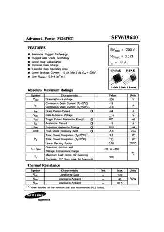
SFW/I9640 Advanced Power MOSFET FEATURES BVDSS = -200 V Avalanche Rugged Technology RDS(on) = 0.5 Rugged Gate Oxide Technology Lower Input Capacitance ID = -11 A Improved Gate Charge Extended Safe Operating Area D2-PAK I2-PAK Lower Leakage Current 10 A (Max.) @ VDS = -200V 2 Low RDS(ON) 0.344 (Typ.) 1 1 2 3 3 1. Gate 2. Drain 3. Source Absolute Maximum
9.6. Size:251K fairchild semi
sfi9620 sfw9620.pdf
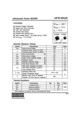
SFW/I9620 Advanced Power MOSFET FEATURES BVDSS = -200 V Avalanche Rugged Technology RDS(on) = 1.5 Rugged Gate Oxide Technology Lower Input Capacitance ID = -3.5 A Improved Gate Charge Extended Safe Operating Area D2-PAK I2-PAK Lower Leakage Current 10 A (Max.) @ VDS = -200V 2 Low RDS(ON) 1.111 (Typ.) 1 1 2 3 3 1. Gate 2. Drain 3. Source Absolute Maximu
9.7. Size:502K samsung
sfw9624.pdf

Advanced Power MOSFET FEATURES BVDSS = -250 V Avalanche Rugged Technology RDS(on) = 2.4 Rugged Gate Oxide Technology Lower Input Capacitance ID = -2.7 A Improved Gate Charge Extended Safe Operating Area Lower Leakage Current 10 A (Max.) @ VDS = -250V 2 Low RDS(ON) 1.65 (Typ.) 1 1 2 3 3 1. Gate 2. Drain 3. Source Absolute Maximum Ratings Symbol Cha
9.8. Size:502K samsung
sfw9634.pdf
Advanced Power MOSFET FEATURES BVDSS = -250 V Avalanche Rugged Technology RDS(on) = 1.3 Rugged Gate Oxide Technology Lower Input Capacitance ID = -5.0 A Improved Gate Charge Extended Safe Operating Area Lower Leakage Current 10 A (Max.) @ VDS = -250V 2 Low RDS(ON) 0.876 (Typ.) 1 1 2 3 3 1. Gate 2. Drain 3. Source Absolute Maximum Ratings Symbol Cha
9.9. Size:504K samsung
sfw9620.pdf

Advanced Power MOSFET FEATURES BVDSS = -200 V Avalanche Rugged Technology RDS(on) = 1.5 Rugged Gate Oxide Technology Lower Input Capacitance ID = -3.5 A Improved Gate Charge Extended Safe Operating Area Lower Leakage Current 10 A (Max.) @ VDS = -200V 2 Low RDS(ON) 1.111 (Typ.) 1 1 2 3 3 1. Gate 2. Drain 3. Source Absolute Maximum Ratings Symbol Ch
9.10. Size:506K samsung
sfw9640.pdf
Advanced Power MOSFET FEATURES BVDSS = -200 V Avalanche Rugged Technology RDS(on) = 0.5 Rugged Gate Oxide Technology Lower Input Capacitance ID = -11 A Improved Gate Charge Extended Safe Operating Area Lower Leakage Current 10 A (Max.) @ VDS = -200V 2 Low RDS(ON) 0.344 (Typ.) 1 1 2 3 3 1. Gate 2. Drain 3. Source Absolute Maximum Ratings Symbol Cha
9.11. Size:501K samsung
sfw9630.pdf

Advanced Power MOSFET FEATURES BVDSS = -200 V Avalanche Rugged Technology RDS(on) = 0.8 Rugged Gate Oxide Technology Lower Input Capacitance ID = -6.5 A Improved Gate Charge Extended Safe Operating Area Lower Leakage Current 10 A (Max.) @ VDS = -200V 2 Low RDS(ON) 0.581 (Typ.) 1 1 2 3 3 1. Gate 2. Drain 3. Source Absolute Maximum Ratings Symbol Ch
Otros transistores... SFU9220
, SFU9224
, SFU9310
, SFW2955
, SFW9510
, SFW9520
, SFW9530
, SFW9540
, IRFP250N
, SFW9614
, SFW9620
, SFW9624
, SFW9630
, SFW9634
, SFW9640
, SFW9644
, SFW9Z14
.
History: G30N04D3
| APT50M50L2FLLG
| ZXMN6A09G
