BSO612CVG MOSFET Equivalente. Reemplazo. Hoja de especificaciones. Principales características
Número de Parte: BSO612CVG
Tipo de FET: MOSFET
Polaridad de transistor: NP
ESPECIFICACIONES MÁXIMAS
Pdⓘ - Máxima disipación de potencia: 2 W
|Vds|ⓘ - Voltaje máximo drenador-fuente: 60 V
|Vgs|ⓘ - Voltaje máximo fuente-puerta: 20 V
|Id|ⓘ - Corriente continua de drenaje: 3 A
Tjⓘ - Temperatura máxima de unión: 150 °C
CARACTERÍSTICAS ELÉCTRICAS
trⓘ - Tiempo de subida: 35 nS
Cossⓘ - Capacitancia de salida: 90 pF
RDSonⓘ - Resistencia estado encendido drenaje a fuente: 0.12 Ohm
Encapsulados: SO-8
Búsqueda de reemplazo de BSO612CVG MOSFET
- Selecciónⓘ de transistores por parámetros
BSO612CVG datasheet
bso612cvg.pdf
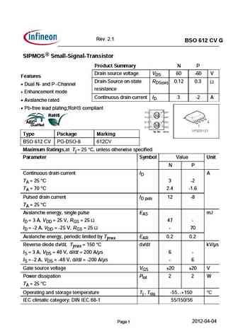
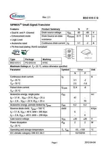
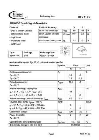
Rev. 2.1 BSO 612 CV G SIPMOS Small-Signal-Transistor Product Summary N P Drain source voltage VDS 60 -60 V Features Drain-Source on-state RDS(on) 0.12 0.3 Dual N- and P -Channel resistance Enhancement mode Continuous drain current ID 3 -2 A Avalanche rated Pb-free lead plating;RoHS compliant Type Package Marking BSO 612 CV PG-DSO-8 612CV Maximum Ratings,at Tj = 25 C, unl
bso612cv.pdf

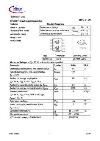
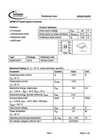
Preliminary data BSO 612 CV SIPMOS Small-Signal-Transistor Features Product Summary N P Drain source voltage VDS 60 -60 V Dual N- and P -Channel Enhancement mode Drain-Source on-state RDS(on) 0.12 0.3 resistance Avalanche rated Continuous drain current ID 3 -2 A dv/dt rated Type Package Ordering Code BSO 612 CV SO 8 Q67041-S4015 Maximum Ratings,at Tj = 25 C, unless otherwi
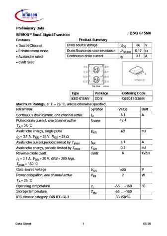
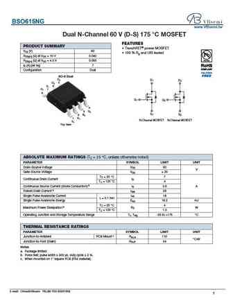
bso615ng.pdf
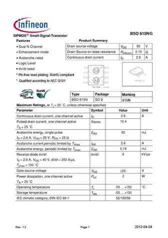
G Pb-free lead plating; RoHS compliant Qualified according to AEC Q101 Marking 615N Rev. 1.2 Page 1 2012-04-04 Rev. 1.2 Page 2 2012-04-04 Rev. 1.2 Page 3 2012-04-04 Rev. 1.2 Page 4 2012-04-04 Rev. 1.2 Page 4 2012-04-04 Rev. 1.2 Page 5 2012-04-04 Rev. 1.4 Page 6 2012-04-04 Rev. 1.2 Page 7 2012-04-04
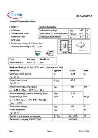
bso615n .pdf
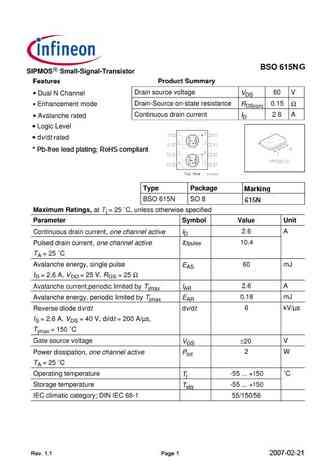
G Pb-free lead plating; RoHS compliant Marking 615N Rev. 1.1 Page 1 2007-02-21 Rev. 1.1 Page 2 2007-02-21 Rev. 1.1 Page 3 2007-02-21 Rev. 1.1 Page 4 2007-02-21 Rev. 1.1 Page 4 2007-02-21 Rev. 1.1 Page 5 2007-02-21 Rev. 1.1 Page 6 2007-02-21 Rev. 1.1 Page 7 2007-02-21
Otros transistores... BSO203P , BSO203SP , BSO207P , BSO211P , BSO220N03MD , BSO301SP , BSO303P , BSO303SP , IRFB3607 , BSO615CG , BSP123 , BSP125 , BSP129 , BSP135 , BSP149 , BSP254A , BSP295 .
🌐 : EN ES РУ

Liste
Recientemente añadidas las descripciónes de los transistores:
MOSFET: AUB062N08BG | AUB060N08AG | AUB056N10 | AUB056N08BGL | AUB050N085 | AUB050N055 | AUB045N12 | AUB045N10BT | AUB039N10 | AUB034N10 | AUB033N08BG | AUB026N085 | AUA062N08BG | AUA060N08AG | AUA056N08BGL | AUA039N10
Popular searches
irfpe50 | tip50 | transistor bc547 datasheet | bc109c | d331 transistor | irfbc40 | mp16b transistor | 2sa934