GP1M011A050XXX Datasheet. Equivalente. Reemplazo. Hoja de especificaciones. Principales características
Número de Parte: GP1M011A050XXX
Tipo de FET: MOSFET
Polaridad de transistor: N
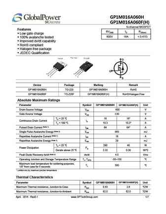
ESPECIFICACIONES MÁXIMAS
Pdⓘ - Máxima disipación de potencia: 158 W
|Vds|ⓘ - Voltaje máximo drenador-fuente: 500 V
|Vgs|ⓘ - Voltaje máximo fuente-puerta: 30 V
|Id|ⓘ - Corriente continua de drenaje: 10 A
Tjⓘ - Temperatura máxima de unión: 150 °C
CARACTERÍSTICAS ELÉCTRICAS
trⓘ - Tiempo de subida: 40 nS
Cossⓘ - Capacitancia de salida: 374 pF
RDSonⓘ - Resistencia estado encendido drenaje a fuente: 0.7 Ohm
Búsqueda de reemplazo de GP1M011A050XXX MOSFET
- Selecciónⓘ de transistores por parámetros
GP1M011A050XXX datasheet
gp1m011a050xxx.pdf
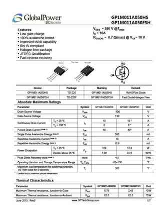
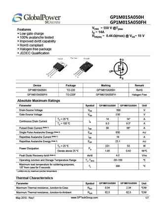
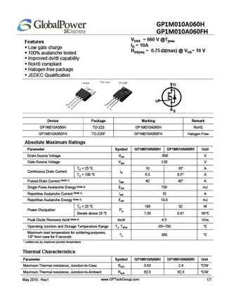
GP1M011A050HS GP1M011A050FSH VDSS = 550 V @Tjmax Features ID = 10A Low gate charge RDS(ON) = 0.7 (max) @ VGS= 10 V 100% avalanche tested Improved dv/dt capability RoHS compliant Halogen free package JEDEC Qualification Fast reverse recovery D G S Device Package Marking Remark GP1M011A050HS TO-220 GP1M011A050HS RoHS/Fast Diode GP1M011A050FSH TO
gp1m011a050xx.pdf
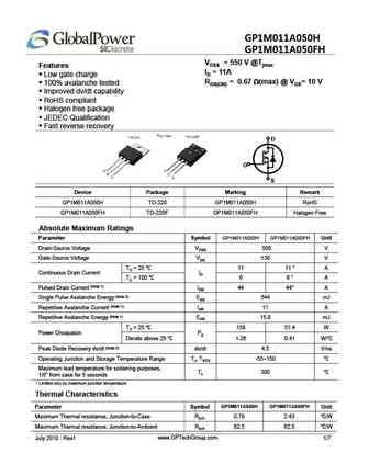
GP1M011A050H GP1M011A050FH VDSS = 550 V @Tjmax Features ID = 11A Low gate charge RDS(ON) = 0.67 (max) @ VGS= 10 V 100% avalanche tested Improved dv/dt capability RoHS compliant Halogen free package JEDEC Qualification Fast reverse recovery D G S Device Package Marking Remark GP1M011A050H TO-220 GP1M011A050H RoHS GP1M011A050FH TO-220F GP1M011A0
gp1m013a050xx.pdf

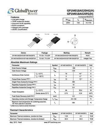
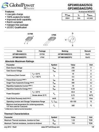
GP1M013A050H GP1M013A050FH VDSS = 550 V @Tjmax Features ID = 13A Low gate charge RDS(on) = 0.48 (max) @ VGS= 10 V 100% avalanche tested Improved dv/dt capability RoHS compliant Halogen free package JEDEC Qualification D G S Device Package Marking Remark GP1M013A050H TO-220 GP1M013A050H RoHS GP1M013A050FH TO-220F GP1M013A050FH Halogen Free Absolute
gp1m018a020xx.pdf
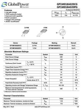
GP1M018A020HG(H) GP1M018A020FG(H) N-channel MOSFET Features Low gate charge BVDSS ID RDS(on)MAX 100% avalanche tested 200V 18A
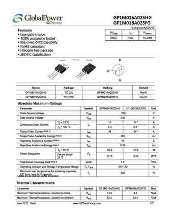
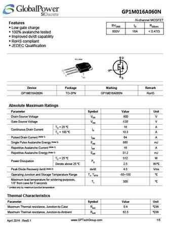
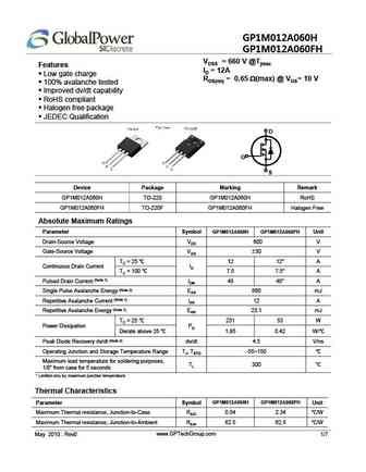

Otros transistores... GP1M009A060XX, GP1M009A070X, GP1M009A090N, GP1M009A090XX, GP1M010A060XX, GP1M010A080N, GP1M010A080XX, GP1M011A050XX, IRF1404, GP1M012A060XX, GP1M013A050XX, GP1M015A050XX, GP1M016A025XG, GP1M016A025XX, GP1M016A060N, GP1M016A060XX, GP1M018A020XG
🌐 : EN ES РУ

Liste
Recientemente añadidas las descripciónes de los transistores:
MOSFET: ASDM30DN30E | ASDM3050KQ | ASDM2305 | ASDM2301 | ASDM2300ZA | ASDM20P13S | ASDM20N90Q | ASDM20N60 | ASDM7002EZA | ASDM68N80KQ | ASDM6802ZC | ASDM60R042NQ | ASDM60P12KQ | ASDM60N80KQ | ASDM60N70Q | ASDM60N50KQ
Popular searches
tip3055 transistor | irf530 datasheet | 2sc2625 | 2sc1815 transistor | 2sd718 | 2n3053 transistor | 2sc458 replacement | bc557 transistor