NCE3401AY MOSFET Equivalente. Reemplazo. Hoja de especificaciones. Principales características
Número de Parte: NCE3401AY
Tipo de FET: MOSFET
Polaridad de transistor: P
ESPECIFICACIONES MÁXIMAS
Pdⓘ - Máxima disipación de potencia: 1.3 W
|Vds|ⓘ - Voltaje máximo drenador-fuente: 30 V
|Vgs|ⓘ - Voltaje máximo fuente-puerta: 12 V
|Id|ⓘ - Corriente continua de drenaje: 4.4 A
Tjⓘ - Temperatura máxima de unión: 150 °C
CARACTERÍSTICAS ELÉCTRICAS
trⓘ - Tiempo de subida: 3 nS
Cossⓘ - Capacitancia de salida: 115 pF
RDSonⓘ - Resistencia estado encendido drenaje a fuente: 0.052 Ohm
Encapsulados: SOT-23
Búsqueda de reemplazo de NCE3401AY MOSFET
- Selecciónⓘ de transistores por parámetros
NCE3401AY datasheet
nce3401ay.pdf
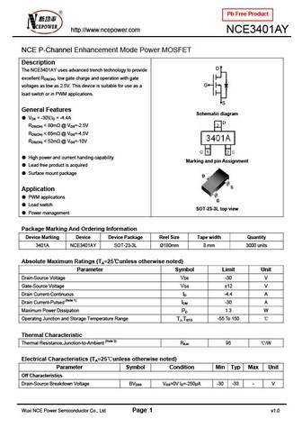
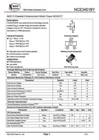
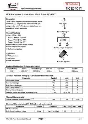
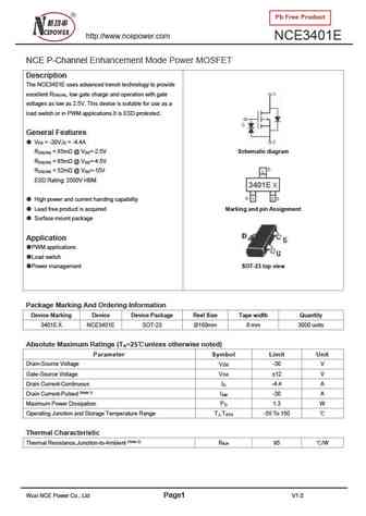
Pb Free Product http //www.ncepower.com NCE3401AY NCE P-Channel Enhancement Mode Power MOSFET Description D The NCE3401AY uses advanced trench technology to provide excellent RDS(ON), low gate charge and operation with gate G voltages as low as 2.5V. This device is suitable for use as a load switch or in PWM applications. S General Features Schematic diagram VDS = -30
nce3401ay.pdf
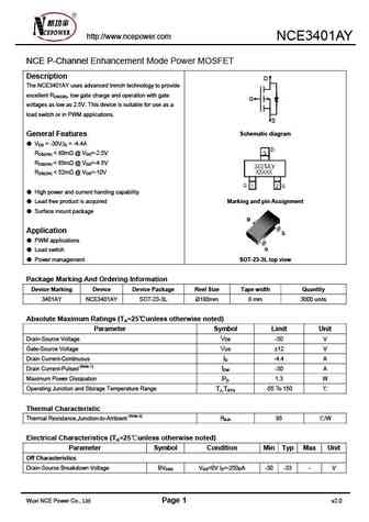
http //www.ncepower.com NCE3401AY NCE P-Channel Enhancement Mode Power MOSFET Description D The NCE3401AY uses advanced trench technology to provide excellent RDS(ON), low gate charge and operation with gate G voltages as low as 2.5V. This device is suitable for use as a load switch or in PWM applications. S Schematic diagram General Features VDS = -30V,ID = -4.4A RD
nce3401a.pdf
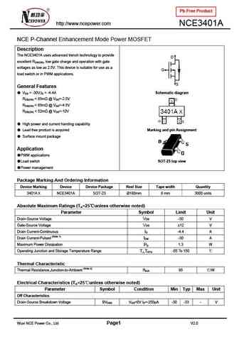
Pb Free Product http //www.ncepower.com NCE3401A NCE P-Channel Enhancement Mode Power MOSFET Description The NCE3401A uses advanced trench technology to provide D excellent RDS(ON), low gate charge and operation with gate voltages as low as 2.5V. This device is suitable for use as a G load switch or in PWM applications. S General Features VDS = -30V,ID = -4.4A Schematic
nce3401.pdf
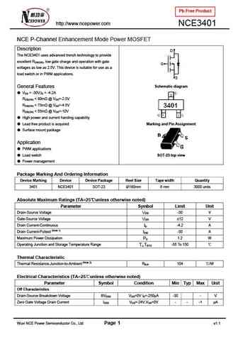
Pb Free Product http //www.ncepower.com NCE3401 NCE P-Channel Enhancement Mode Power MOSFET Description D The NCE3401 uses advanced trench technology to provide excellent RDS(ON), low gate charge and operation with gate G voltages as low as 2.5V. This device is suitable for use as a load switch or in PWM applications. S Schematic diagram General Features VDS = -30V,ID
Otros transistores... JCS4N60RB , JCS4N60BB , JCS4N60CB , JCS4N60FB , LD1014D , ME80N75F , ME80N75FG , MMF60R280QTH , AOD4184A , NDF08N60ZG , NDP08N60ZG , PTF10149 , RJK0234DNS , SPP100N06S2-05 , SPB100N06S2-05 , SSM5N03FE , STK0260D .
History: 60N10B | DH012N03I
🌐 : EN ES РУ

Liste
Recientemente añadidas las descripciónes de los transistores:
MOSFET: AUB034N10 | AUB033N08BG | AUB026N085 | AUA062N08BG | AUA060N08AG | AUA056N08BGL | AUA039N10 | ASW80R290E | ASW65R120EFD | ASW65R110E | ASW65R095EFD | ASW65R046EFD | ASW65R041EFDA | ASW65R041E | ASW60R150E | ASW60R090EFDA
Popular searches
mpsa20 | irfp264 | ksc2690 | bc546 datasheet | mpsa06 transistor | tta004b | 2sc1116 | 2n3565 equivalent