NCE3401AY Specs and Replacement
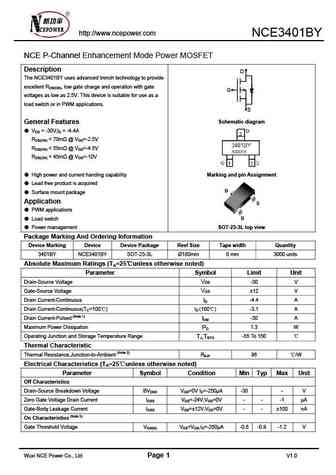
Type Designator: NCE3401AY
Type of Transistor: MOSFET
Type of Control Channel: P-Channel
Absolute Maximum Ratings
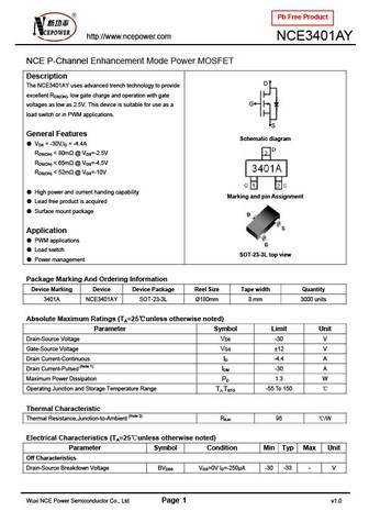
Pd ⓘ - Maximum Power Dissipation: 1.3 W
|Vds|ⓘ - Maximum Drain-Source Voltage: 30 V
|Vgs|ⓘ - Maximum Gate-Source Voltage: 12 V
|Id| ⓘ - Maximum Drain Current: 4.4 A
Tj ⓘ - Maximum Junction Temperature: 150 °C
Electrical Characteristics
tr ⓘ - Rise Time: 3 nS
Cossⓘ - Output Capacitance: 115 pF
RDSonⓘ - Maximum Drain-Source On-State Resistance: 0.052 Ohm
Package: SOT-23
NCE3401AY substitution
- MOSFET ⓘ Cross-Reference Search
NCE3401AY datasheet
nce3401ay.pdf
Pb Free Product http //www.ncepower.com NCE3401AY NCE P-Channel Enhancement Mode Power MOSFET Description D The NCE3401AY uses advanced trench technology to provide excellent RDS(ON), low gate charge and operation with gate G voltages as low as 2.5V. This device is suitable for use as a load switch or in PWM applications. S General Features Schematic diagram VDS = -30... See More ⇒
nce3401ay.pdf
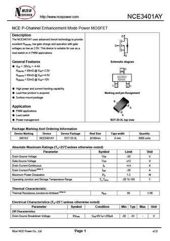
http //www.ncepower.com NCE3401AY NCE P-Channel Enhancement Mode Power MOSFET Description D The NCE3401AY uses advanced trench technology to provide excellent RDS(ON), low gate charge and operation with gate G voltages as low as 2.5V. This device is suitable for use as a load switch or in PWM applications. S Schematic diagram General Features VDS = -30V,ID = -4.4A RD... See More ⇒
nce3401a.pdf
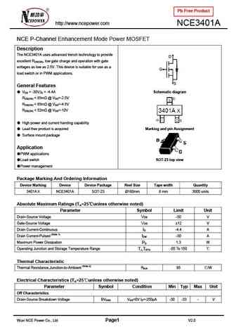
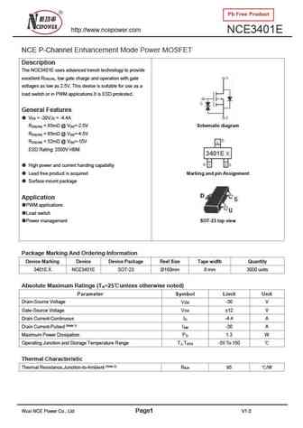
Pb Free Product http //www.ncepower.com NCE3401A NCE P-Channel Enhancement Mode Power MOSFET Description The NCE3401A uses advanced trench technology to provide D excellent RDS(ON), low gate charge and operation with gate voltages as low as 2.5V. This device is suitable for use as a G load switch or in PWM applications. S General Features VDS = -30V,ID = -4.4A Schematic... See More ⇒
nce3401.pdf
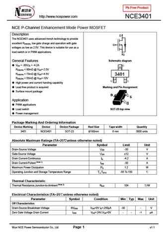
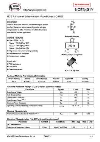
Pb Free Product http //www.ncepower.com NCE3401 NCE P-Channel Enhancement Mode Power MOSFET Description D The NCE3401 uses advanced trench technology to provide excellent RDS(ON), low gate charge and operation with gate G voltages as low as 2.5V. This device is suitable for use as a load switch or in PWM applications. S Schematic diagram General Features VDS = -30V,ID... See More ⇒
Detailed specifications: JCS4N60RB, JCS4N60BB, JCS4N60CB, JCS4N60FB, LD1014D, ME80N75F, ME80N75FG, MMF60R280QTH, AOD4184A, NDF08N60ZG, NDP08N60ZG, PTF10149, RJK0234DNS, SPP100N06S2-05, SPB100N06S2-05, SSM5N03FE, STK0260D
Keywords - NCE3401AY MOSFET specs
NCE3401AY cross reference
NCE3401AY equivalent finder
NCE3401AY pdf lookup
NCE3401AY substitution
NCE3401AY replacement
Can't find your MOSFET? Learn how to find a substitute transistor by analyzing voltage, current and package compatibility
History: WML15N65F2 | FDD6644 | FDB3632
🌐 : EN ES РУ
LIST
Last Update
MOSFET: AUB034N10 | AUB033N08BG | AUB026N085 | AUA062N08BG | AUA060N08AG | AUA056N08BGL | AUA039N10 | ASW80R290E | ASW65R120EFD | ASW65R110E
Popular searches
mpsa20 | irfp264 | ksc2690 | bc546 datasheet | mpsa06 transistor | tta004b | 2sc1116 | 2n3565 equivalent
